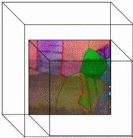
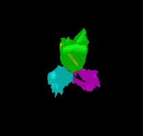
3D EBSD - tomographic analysis of complex microstructures
Here are some results on the 3D high resolution characterisation of crystalline microstructures. The technique is based on automated serial sectioning using a focused ion beam (FIB) and characterisation of the sections by orientation microscopy based on electron backscatter diffraction (EBSD) in a combined FIB-scanning electron microscope (SEM). On our system, consisting of a Zeiss Crossbeam FIB-SEM and a TSL/EDAX EBSD system the technique currently reaches a spatial resolution of 100 x 100 x 100 nm³ as a standard but a resolution of 50 x 50 x 50 nm³ seems to be a realistic optimum. The maximum observable volume is in the order of 50 x 50 x 50 µm³. The technique shows all the powerful features of 2-dimensional EBSD-based orientation microscopy and extends them into the third dimension of space. This allows new parameters about the microstructure to be obtained, for example the full crystallographic characterisation of all kinds of interfaces, including the morphology and the crystallographic indices of the interface planes.
 3D EBSD: Max-Planck Institut für Eisenforschung Düsseldorf
Overview of 3D EBSD: Three-Dimensional Orientation Microscopy in a Focused Ion Beam–Scanning Electron Microscope: A New Dimension of Microstructure Characterization
Here we report on our progress in the development, optimization, and application of a technique for the three-dimensional (3-D) high-resolution characterization of crystalline microstructures.
3D EBSD overview Metall Mater Trans A vo[...]
PDF-Dokument [1.0 MB]
Ultra Fine Grained CuZr Alloy Processed by Equal Channel Angular Pressing
AEM_3D-EBSD_2011.pdf
PDF-Dokument [760.9 KB]
Three-dimensional EBSD study on the relationship between triple junctions and columnar grains in electrodeposited Co–Ni films
Journal of Microscopy 230 (2008) 487–498[...]
PDF-Dokument [667.5 KB]
 page 374 vol 39A, 2008 METALLURGICAL AND MATERIALS TRANSACTIONS A
3D EBSD methodology that enables the measurement of all five degrees of freedom of grain boundaries (GBs) combined with segregation analysis using atom probe tomography.
2014 scripta Mandal GB segregation 3D EB[...]
PDF-Dokument [972.8 KB]
Crystal plasticity polycrystal model of the structure evolution and the mechanical behavior of a Mo–TiC30 vol.% metal–ceramic composite
Acta-Mater-2012-Mo-TiC.pdf
PDF-Dokument [1.6 MB]
Here we investigate orientation gradients and geometrically necessary dislocations (GNDs) in two ultrafine grained dual-phase steels (DP steels) with different martensite particle size and volume frac
Mater_Science_Engin_A 527 (2010) 2738.pd[...]
PDF-Dokument [2.2 MB]
Acta Materialia 57 (2009) 559 indent.pdf
PDF-Dokument [1.9 MB]
Raabe Acta Materialia 54 (2006) 1863.pdf
PDF-Dokument [1.5 MB]
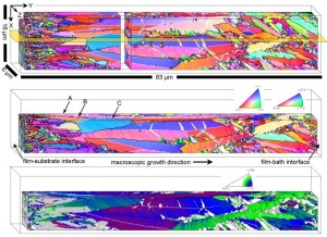
3D EBSD on diamond thin film layers
3D EBSD diamond-stam8_3_035013.pdf
PDF-Dokument [1.1 MB]
2D EBSD: Microtexture and Grain Boundaries in Freestanding CVD Diamond Films: Growth and Twinning Mechanisms
Adv Funct Mater 2009 Vol 19 page 3880–38[...]
PDF-Dokument [2.1 MB]