Semiconductors and Solar cell materials studied by Atom Probe Tomography
Grain boundaries in materials have substantial influences on device properties, for instance on mechanical stability or electronic minority carrier lifetime in multicrystalline silicon solar cells. This applies especially to asymmetric, less ordered or faceted interface portions. Here, we present the complex atomic interface structure of an asymmetric Σ9 tilt grain boundary in silicon, observed by high resolution scanning transmission electron microscopy (HR-STEM) and explained by atomistic modeling and computer simulation. Structural optimization of interface models for the asymmetric Σ9 and related symmetrical Σ9 and Σ3 tilt grain boundaries, by means of molecular-statics simulations with empirical silicon potentials in combination with first-principles calculations, results in a fac
PRL vol 115 (2015) 235502 Complex Nanotw[...]
PDF-Dokument [1.3 MB]
 EBIC map of the studied sample area in correlation with the CSL character obtained by EBSD (RGB). The arrow indicates the analyzed triple junction. (b) Overview of the TEM specimen containing a triple junction of two Σ3 and one Σ9 GBs.
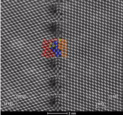 HR-STEM image of an asymmetric Σ9 111 115 boundary of two Si grains in the [110] projection. The period of the complex GB structure is indicated by white dashed lines.
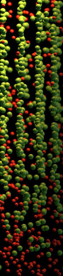
 Relaxed atomic structure model of the faceted Σ9 111 115 GB viewed along the [110] direction. Red spheres and orange spheres depict the two different grains. The facet is colored in blue, while yellow balls represent single atom columns.
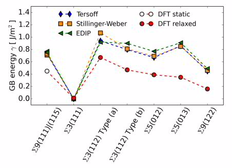 Calculated GB energies for various GBs. DFT values are taken from Ref. [24]. The DFT value of the GB energy for the asymmetric Σ9ð111Þjð115Þ has been obtained from a static calculation using the relaxed structure as obtained by empirical potentials.
APPLIED PHYSICS LETTERS 107, 172102 (2015)
APPLIED PHYSICS LETTERS 107, 172102 (201[...]
PDF-Dokument [944.0 KB]
Kesterite structured compound semiconductors Cu2ZnSn (S,Se) (CZTSSe) are of rapidly growing interest as materials for photovoltaic applications.
These compounds exhibit high absorption coefficients as well as direct energy band gaps (1–1.5 eV) and comprise low cost, non-toxic, and earth abundant elements. Thus, CZTSSe
films are considered as highly promising absorbers for thin-film solar cells. The current record energy conversion efficiency of CZTSSe-based
solar cells is 12.6%, which is still far below that of chalcopyrite compounds Cu(In,Ga)(S,Se) (21.7%). One of the main reasons for the limited performance of CZTSSe solar cells is
the difficulty to prepare single phase CZTSSe without the formation of secondary phases. Both theoretical and experimental data show that CZTSSe compounds have a very narrow
existence region, with only 1%–2% absolute deviation from nominal stoichiometry. Moreover, evaporation of volatile S(e) and SnS(e)and the presence of a reactive Mo back contact can cause the
decomposition of CZTSSe into secondary phases.
Several secondary phases have been reported for CZTSSe thin-films such as ZnS(e),CuxS(e), Cu2SnS(e)3, and SnS(e)x. Secondary phases are generally considered to be detrimental to cell
efficiency, as they increase the recombination rates and consequently cause a loss in open circuit voltage and/or can lead to an increase in series resistance. Hence,
reliable and accurate characterization of the secondary phase precipitates with respect to their composition, size, and spatial distribution within the absorber is essential for understanding the
solar cell properties and controlling the synthesis and process parameters. Detection of secondary phases remains a great challenge, as many of them are structurally similar to the
CZTSSe matrix and are formed as nanosized precipitates. Recently, we reported on the detection of a complex network of nanometer-sized ZnSe grains within a CZTSe absorber layer22 using atom probe tomography (APT).
The absorber had been prepared by the low-temperature co-evaporation of a precursor (320°C substrate temperature), followed by etching in a KCN-solution and post-deposition annealing at 500°C. APT
analyses of this absorber also revealed that some of the detected ZnSe grains contained Cu- and Sn-rich precipitates, which could not be attributed to any known equilibrium phase. However, it was not
possible to clearly understand the complex atomic-scale processes occurring during absorber fabrication.
Here, Cu2ZnSnSe4 thin-films for photovoltaic applications are investigated using combined atom probe tomography and ab initio
density functional theory. The atom probe studies reveal nano-sized grains of Cu2Zn5SnSe8 and Cu2Zn6SnSe9 composition, which cannot be assigned to any known phase reported in the
literature. Both phases are considered to be metastable, as density functional theory calculations yield positive energy differences with respect to the decomposition into Cu2ZnSnSe4 and
ZnSe. Among the conceivable crystal structures for both phases, a distorted zincblende structure shows the lowest energy, which is a few tens of meV below the energy of a wurtzite structure. A band
gap of 1.1 eV is calculated for both the Cu2Zn5SnSe8 and Cu2Zn6SnSe9 phases. Possible effects of these phases on solar cell performance are discussed.
Ultramicroscopy 156 (2015) 29-36
Ultramicroscopy-156-(2015)-29-Al In Ga N[...]
PDF-Dokument [2.0 MB]
The electronic properties of quaternary AlInGaN devices significantly depend on the homogeneity of the alloy. The identification of compositional fluctuations or verification of random-alloy distribution is hence of grave importance. Here, a comprehensive multiprobe study of composition and compositional homogeneity is presented, investigating AlInGaN layers with indium concentrations ranging from 0 to 17 at% and aluminium concentrations between 0 and 39 at% employing high-angle annular dark field scanning electron microscopy (HAADF STEM), energy dispersive X-ray spectroscopy (EDX) and atom probe tomography (APT). EDX mappings reveal distributions of local concentrations which are in good agreement with random alloy atomic distributions. This was hence investigated with HAADF STEM by comparison with theoretical random alloy expectations using statistical tests. To validate the performance of these tests, HAADF STEM image simulations were carried out for the case of a random-alloy distribution of atoms and for the case of In-rich clusters with nanometer dimensions. The investigated samples, which were grown by metal-organic vapor phase epitaxy (MOVPE), were thereby found to be
homogeneous on this nanometer scale. Analysis of reconstructions obtained from APT measurements yielded matching results. Though HAADF STEM only allows for the reduction of possible
combinations of indium and aluminium concentrations to the proximity of isolines in the two-dimensional composition
space. The observed ranges of composition are in good agreement with the EDX and APT results within the respective precisions.
17th International Conference on Microscopy of Semiconducting Materials 2011
IOP Publishing Journal of Physics: Conference Series 326 (2011) 012029
doi:10.1088/1742-6596/326/1/012029
Journal-of-Physics_ConfSeries_326_012029[...]
PDF-Dokument [2.0 MB]
In this work we show how the indium concentration in high indium content
InxGa1-xN quantum wells, as they are commonly used in blue and green light emitting diodes, can be deduced from high-angle annular dark-field scanning transmission electron
microscopy (HAADF-STEM) images. This method bases on introducing normalized intensities which can be compared with multislice simulations to determine the specimen thickness or the
indium concentration. The evaluated concentrations are compared with atom probe tomography
measurements. It is also demonstrated how the quality of focused ion beam prepared TEM lamellas can be improved by an additional etching with low energy ions.
APPLIED PHYSICS LETTERS 102, 132112 (2013)
Atom Probe InGaN layers APL 2013 Mehrten[...]
PDF-Dokument [1.7 MB]
A method for determining concentrations from high-angle annular dark field-scanning transmission electron microscopy images is presented. The method is applied to an InGaN/GaN
multi-quantum well structure with high In content, as used for the fabrication of light emitting diodes and laser diodes emitting in the green spectral range. Information on specimen
thickness and In concentration is extracted by comparison with multislice calculations. Resulting concentration
profiles are in good agreement with a comparative atom probe tomography analysis. Indium concentrations in the quantum wells ranging from 26
at.% to 33 at.% are measured in both cases.
Prog. Photovolt: Res. Appl. (2015)
Grain boundary segregation in multicrystalline silicon: correlative characterization by EBSD, EBIC, and atom probe tomography
Andreas Stoffers, Oana Cojocaru-Mirédin, Winfried Seifert, Stefan Zaefferer,
Stephan Riepe and Dierk Raabe
Stoffers PROGRESS IN PHOTOVOLTAICS GB se[...]
PDF-Dokument [1.0 MB]
 Prog. Photovolt: Res. Appl. (2015) Grain boundary segregation in multicrystalline silicon: correlative characterization by EBSD, EBIC, and atom probe tomography Andreas Stoffers, Oana Cojocaru-Mirédin, Winfried Seifert, Stefan Zaefferer, et al.


Multicrystalline silicon (mc-Si) is a commonly used and highly cost-effective
bulk material for solar cell applications [1]. Up to date, the record efficiency registered for mc-Si solar cells is 20.8%, while the one registered for monocrystalline Si solar cells
is 25.6% [2]. Contrary to monocrystalline Si,
mc-Si contains high densities of defects, such as dislocations, grain boundaries (GBs), and stacking faults, reducing the solar cell efficiency [1]. The model developed by Kveder et
al. [3] explains how the recombination rate of
the minority charge carriers increases when dislocations are contaminated by transition metal impurities. Because of advanced crystallization techniques, the density of
dislocation clusters in mc-Si has been significantly reduced
such that the recombination at GBs comes into focus again [4]. For recombination at GBs, no equivalent model for the effects of the impurities on the GBs recombination rates exists
[5]. This may be due to generally complex crystallographic structure of GBs, characterized by its misorientation
and plane inclination [6]. It has been suggested though that the presence of transition metal impurities at Si GBs
may create deep levels, which induce a higher recombination activity. The main effect is a decrease of
the average minority carrier lifetime, which is directly linked with the solar cell efficiency [7]. C and O are
well-known impurity species in mc-Si, inherited from the crystallization furnace and the
crucible [8]. According to the Gibbs adsorption isotherm, such
impurities will segregate to defects, particularly to GBs [9,10]. Only few studies exist though on the impact of these light GB impurities on the recombination activity [11],
whereas vast literature exists on the detrimental effects of transition metals, such as Fe, Cr, Ni, and Cu, on the carrier recombination and cell efficiency [12–16]. The critical bulk
concentration has been reported to be in the range of 1014 at/cm3 for Fe and Cu [13]. Electron-beam-induced current (EBIC) studies suggest that the recombination activity is different
from one GB to another [17,18]. Even more remarkable is the fact that the EBIC contrast can change along the same GB [17,19,20]. During the last years, it has been shown
that transition metal impurities and light elements segregate mainly at the GBs in the form of heterogeneous precipitates as silicides (such as FeSi2 [21], NiSi2 [22], and Cu3Si
[13]), carbides (SiC), and oxides (SiO2). The presence of these precipitates induces supplementary strong dot-like dark features in EBIC maps mainly at the GBs but cannot alone explain
the complexity of the EBIC maps such as recombination-free segments and contrast variations observed along some of the GBs [17]. These early observations clearly show that a
complex
relationship exists between the crystallographic character of GBs, the type of impurity element segregated to them, and their recombination rates. For this reason, we conducted a
systematic analysis of GBs using correlative electron
backscatter diffraction (EBSD)–EBIC–atom probe tomography (APT) measurements. The precise correlation requires a challenging site-specific sample preparation. A special sample holder
system was developed, which enables us to mount the samples in all the involved microscopes (scanning electron microscope (SEM), focused ion beam (FIB), transmission electron
microscope (TEM), EBSD, EBIC, and APT) without changing the retainer
and thus facilitates the sample preparation [23,24]. Therefore, a better understanding of corresponding structure-property relationships in mc-Si solar cells is expected, by coupling
the local chemistry with the GB type and electrical
activity. Moreover, the present 3D APT study is the first correlative EBSD–EBIC–APT study and one of the first direct identification and quantification experiments of impurities
decorating GBs in mc-Si [25,26].
This study aims to better understand the influence of crystallographic structure and impurity decoration on the recombination activity at grain boundaries in multicrystalline silicon. A
sample of the upper part of a multicrystalline silicon ingot with intentional addition of iron and copper has been investigated. Correlative electron-beam-induced current,
electron backscatter diffraction, and atom probe tomography data for different types of grain boundaries are presented. For a symmetric coherent Σ3 twin boundary, with very low
recombination activity, no impurities are detected. In case of a non-coherent
(random) high-angle grain boundary and higher order twins with pronounced recombination activity, carbon and oxygen impurities are observed to decorate the interface. Copper contamination is
detected for the boundary with the highest recombination activity in this study, a random high-angle grain boundary located in the vicinity of a triple junction. The 3D atom probe
tomography study presented here is the first direct atomic scale identification and quantification of
impurities decorating grain boundaries in multicrystalline silicon. The observed deviations in chemical decoration and induced current could be directly linked with different crystallographic
structures of silicon grain boundaries. Hence, the current work establishes a direct correlation between grain boundary structure, atomic scale segregation information, and electrical
activity. It can help to identify interface–property relationships for silicon interfaces that enable grain boundary
engineering in multicrystalline silicon.