EBSD - Electron Back-Scatter Diffraction
What is EBSD - Electron Back-Scatter Diffraction?
Electron Back-Scatter Diffraction (EBSD), which is sometimes also referred to as Backscatter Kikuchi Diffraction (BKD) is a typcially SEM-based backscatter or
transmission electron diffraction technique for retrieving crystallographic orientation and phase information from crystalline materials.
Typcially such experiments are conducted in the scanning electron microscope (SEM) or in cross beam FIB-SEM instruments.
EBSD yields information on the crystallographic nature of the illuminated phase and / or the crystallographic orientation of crystals with a spatial resolution of a few
microns down to a few nanometer for instance when using
field emission SEM systemsat low current density and / or operating in transmission mode.
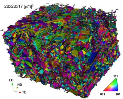
 Dual phase steel microstructure revealed by 3D EBSD.
The method is based on obtaining maps of Electron Back-Scatter Patterns of individual crystalline regions.
EBSP's consist of symmetrically arranged bands which are referred to as Kikuchi or pseudo Kikuchi or backscatter Kikuchi bands of slightly higher intensity with respect to a non-uniform background. This contrast is due to the diffraction of the backscattered electrons by the crystal. Those electrons, generated by an incident electron beam in the SEM, spread beneath the specimen surface in all directions. This produces a divergent source of electrons within an interaction volume in the sample, which will diffract with the crystal planes according to the Bragg condition. Because the electrons travel from the source in all directions, for each set of planes for which the Bragg condition is satisfied, the diffracted beams lie on the surface of a cone whose axis is normal to the diffracted plane. Those cones intersect with a phosphor screen placed in front of the specimen and give rise to the patterns.
 Through-thickness hot band texture of ferritic steel
 High resolution EBSD on a maraging TRIP steel (Scripta Materialia 60 (2009) 1141)
What is 3D EBSD / EBSD tomography ?
3D EBSD which is sometimes also referrd to as EBSD tomography is a 3D-orientation microscopy method that works by sequential serial sectioning in a FIB-SEM, by serial polishing or sequential layer
ablation by Laser.
We mainly use a technique that is based on automated serial sectioning using a focused ion beam (FIB) and characterisation of the sections by orientation microscopy based on electron backscatter
diffraction (EBSD) in a combined FIB-scanning electron microscope (SEM). On our system, consisting of a Zeiss Crossbeam FIB-SEM and an EDAX-TSL EBSD system the technique currently reaches a spatial
resolution of 100 x 100 x 100 nm³ as a standard but a resolution of 50 x 50 x 50 nm³ seems to be a realistic optimum. The maximum observable volume is in the order of 50 x 50 x 50 µm³. The technique
shows all the powerful features of 2-dimensional EBSD-based orientation microscopy and extends them into the third dimension of space. This allows new parameters about the microstructure to be
obtained, for example the full crystallographic characterisation of all kinds of interfaces, including the morphology and the crystallographic indices of the interface planes. The technique is
illustrated by 4 examples, including the characterisation of pearlite colonies in a carbon steel, of twins in pseudo-nanocrystalline NiCo thin films, the description of deformation patterns formed
under nano-indents in copper single crystals and the characterisation of fatigue cracks in an aluminium alloy. Besides the description of our own system we give an extensive overview on parallel
developments of 3D orientation microscopy (with a focus on the EBSD-based techniques) in other groups and discuss the possibilities and limits of the technique.
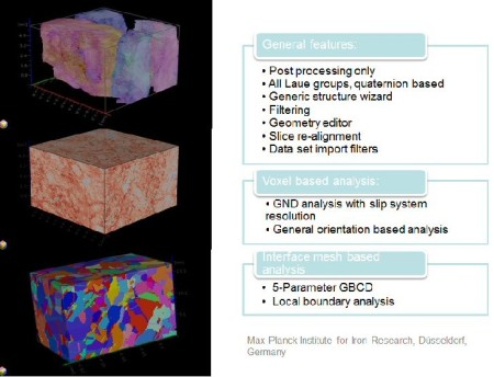
 3D EBSD (EBSD tomography) enabling full crystallographic characterization of materials interfaces
SEM-based EBSD has become a dominant method in physical metallurgy and is used as the new gold standard in modern metallography. It allows us to quantify phases, textures, and internal substructures in complex engineering and functional materials.
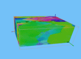
Example of 3D EBSD: 3D Grain boundary plane analysis in CdTe solar cell absorber layers
This study is on the microstructure, crystallographic texture and its evolution during processing of CdTe absorber layers from CdTe/CdS thin film solar cells grown by low-temperature processes in substrate configuration. Investigations were performed at different stages of the cell manufacturing, from deposition to the final functional solar cell, with the aim to understand the microstructure formation of the photoactive layer. To this end 3-dimensional microstructure characterization was performed using focused ion beam/electron backscatter diffraction tomography ("3D-EBSD") together with conventional 2D-EBSD. The analyses revealed strong microstructural and textural changes developing across the thickness of the absorber material, between the back contact and the p–n junction interfaces. Based on the 3-dimensional reconstruction of the CdTe thin film, a coherent growth model was proposed, emphasizing the microstructural continuity before and after a typical CdCl2-annealing activation treatment. One of the principal results is that the absorber layer is created by two concomitant processes, deposition and recrystallization, which led to different textures and microstructures. Further changes are the result of subsequent annealing treatments, favoring twinning and promoting well-defined texture components. The results open the possibility for a grain boundary engineering approach applied to the design of such cells.
Solar Energy Materials & Solar Cells 151 (2016) 66-80
Solar Energy Materials Solar Cells vol 5[...]
PDF-Dokument [2.4 MB]
 3-Dimensionnal EBSD reconstruction of the as-deposited layer, (b) large grains developing from the back contact interface and (c) part of the fine-grained matrix present close to the p–n junction interface.
How to determine geometrically necessary dislocation patterns by 3D EBSD ?
Stored dislocations are generally divided into geometrically necessary dislocations (GNDs), which accommodate a lattice curvature from a deformation gradient, and statistically
stored dislocations (SSDs), which accumulate due to statistical entanglements. The focus of this work is entirely on the class of
GNDs. As GNDs are the result of a deformation process, they are mainly a measure for differences in plastic flow and they contribute to the stored energy and strain hardening during
cold working.
Nye, Kröner and Bilby established a continuum dislocation theory that provides the connection between the lattice curvature and a continuous GND distribution. Sun et al. were the first
to apply this theory with the help of electron backscatter diffraction (EBSD) to resolve GND distributions in Al bicrystals. Since then, a range of studies into GND distributions have
been performed, all based on employing conventional EBSD pattern analysis by Hough transform. More recently, EBSD pattern cross correlation has been applied to obtain more accurate
lattice rotation and GND results. As most GND studies are based on 2-dimensional EBSD measurements, they consequently deal with the missing out-of-plane components in Nye’s
dislocation tensor in various ways. Recent advancements, by solving an additional static stress equilibrium condition, have led to a complete (but still surface based) dislocation
tensor, though [20]. The current work is entirely based on 3D EBSD measurements and therefore neither limited by an incomplete Nye tensor nor by a missing dimension in the GND density
field. Our 3D EBSD measurements are performed by serial sectioning with a focussed Ga+-ion beam and a subsequent mapping of the consecutive sections by EBSD. The number of methods to
map dislocation densities by other means is rather limited and includes methods such as direct observations by electron channelling contrast imaging (ECCI) and transmission electron
microscopy or indirect observations by etch pits or X-ray diffraction profile analysis. This and the difficulty to differentiate between GNDs and SSDs is probably the main reason why
there have been only very few attempts so far to compare the outcome of GND calculations with direct measurements of dislocation densities.
In the present work we attempt to verify the density of GNDs obtained by 3D EBSD on the basis of an experiment which creates an analytically quantifiable amount of GNDs. We use a
constrained micro-cantilever bending experiment, assuming that the GND density can be calculated from an experimentally determinable bending radius. Provided that the deformation is
carried mainly
by GNDs, this will be a suitable set-up to relate GND densities to the plastic deformation gradient.
Acta Materialia 99 (2015) 402-414
Assessment of geometrically necessary dislocation levels derived by 3D EBSD
P.J. Konijnenberg, S. Zaefferer, D. Raabe
Acta Mater 99 (2015) 402 - 3D EBSD Geoem[...]
PDF-Dokument [2.7 MB]
 Acta Materialia 99 (2015) 402: Assessment of geometrically necessary dislocation levels derived by 3D EBSD P.J. Konijnenberg, S. Zaefferer, D. Raabe
A. Khorashadizadeh, D. Raabe, S. Zaefferer, G. S. Rohrer, A. D. Rollett, M. Winning
ADVANCED ENGINEERING MATERIALS 2011, 13, No. 4
AEM_3D-EBSD_2011.pdf
PDF-Dokument [760.9 KB]
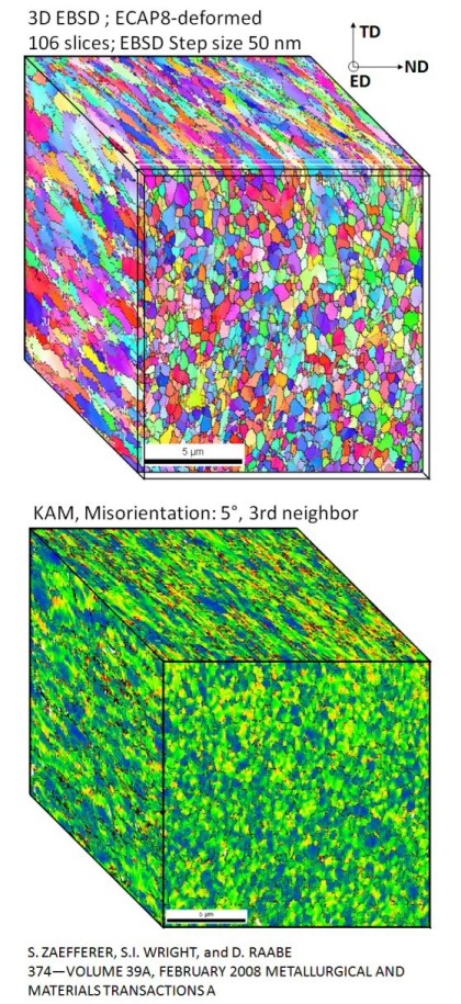
The 3D grain boundary character distribution (GBCD) of a sample subjected to equal channel angular pressing (ECAP) after eight passes and successive annealing at 650 8C for about 10 min is
analyzed. The experiments are conducted using a dual beam system, which is a combination of a focused ion beam and a scanning electron microscope to collect a series of electron backscatter
diffraction (EBSD) maps of the microstructure (3D EBSD). The data set was aligned and reconstructed to a 3D microstructure. The crystallographic character of the grain boundary planes was
determined using three different
methods, namely, the line segment method, the stereological method, and the triangular surface mesh method. The line segment and triangular surface mesh methods produce consistent data sets,
both yielding approximately a 7% area fraction of coherent twins. These results starkly contrast that of the statistical stereological method, which produced a 44% area fraction of coherent
twins.
3D EBSD
 Khorashadizadeh, Raabe, Zaefferer, Rohrer, Rollett, Winning: Adv. Engin. Mater. 13 (2011) 237
Besides the conventional 2D EBSD approach we also a technique for the 3-dimensional EBSD-based tomographic high resolution characterisation of crystalline microstructures (3D EBSD). The technique is based on automated serial sectioning using a focused ion beam (FIB) and characterisation of the sections by orientation microscopy based on electron backscatter diffraction (EBSD) in a combined FIB-scanning electron microscope (SEM). On our system, consisting of a Zeiss Crossbeam FIB-SEM and a TSL/EDAX EBSD system the technique currently reaches a spatial resolution of 50 x 50 x 50 nm³ as a standard resolution. The observable volume is in the order of 50 x 50 x 50 µm³. The technique shows all the powerful features of 2D EBSD-based orientation microscopy and extends them into the third dimension of space. This allows new parameters about the microstructure to be obtained, for example the full crystallographic characterisation of all kinds of interfaces, including the morphology and the crystallographic indices of the interface planes.
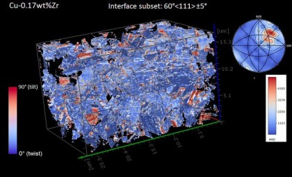
 Interfaces obtained by a 3D EBSD analysis on Cu
3D EBSD : 3D-orientation microscopy in a FIB SEM
Here we report about recent progress in development and optimisation of a technique for the 3-dimensional high resolution characterisation of crystalline microstructures, referred to as 3D EBSD. The technique is based on automated serial sectioning using a focused ion beam (FIB) and characterisation of the sections by orientation microscopy based on electron backscatter diffraction (EBSD) in a combined FIB-scanning electron microscope (SEM). On our system, consisting of a Zeiss Crossbeam FIB-SEM and an EDAX-TSL EBSD system the technique currently reaches a spatial resolution of 100 x 100 x 100 nm³ as a standard but a resolution of 50 x 50 x 50 nm³ seems to be a realistic optimum. The maximum observable volume is in the order of 50 x 50 x 50 µm³. The technique shows all the powerful features of 2-dimensional EBSD-based orientation microscopy and extends them into the third dimension of space. This allows new parameters about the microstructure to be obtained, for example the full crystallographic characterisation of all kinds of interfaces, including the morphology and the crystallographic indices of the interface planes. The technique is illustrated by 4 examples, including the characterisation of pearlite colonies in a carbon steel, of twins in pseudo-nanocrystalline NiCo thin films, the description of deformation patterns formed under nano-indents in copper single crystals and the characterisation of fatigue cracks in an aluminium alloy. Besides the description of our own system we give an extensive overview on parallel developments of 3D orientation microscopy (with a focus on the EBSD-based techniques) in other groups and discuss the possibilities and limits of the technique.
1 Introduction
1.1 Motivation: why perform 3D investigations?
Metallographic techniques for the characterisation of microstructures of materials are usually applied to 2-dimensional planes cut through a sample. In many cases, this is sufficient. Statistical
stereological techniques can be used to gain insight into the 3 dimensional aspects of microstructure [1][2]. However, there are also a large number of cases where a true 3 dimensional
characterisation of a sample volume is critical to a correct understanding of the role the microstructure plays in a particular material property. Cases where three-dimensional (3D) information is of
great importance are, for example, the true size and shape of grains for grain growth investigations, the size and shape of strain fields for studies on deformation or the distribution and position
of nuclei for recrystallisation investigations. Information that is completely missing in two-dimensional (2D) microstructure observations is the full crystallographic characterisation of grain or
phase boundaries. In two-dimensional orientation microscopy the misorientation across a boundary can be determined; however, since the spatial orientation of the boundary plane is unknown, the
orientation of the boundary plane relative to the crystal lattices separated by the plane cannot be determined. This information is of great importance for the investigation of phase transformations,
grain growth processes or intergranular fracture.
Principally, 3D-characterisation of microstructures can be performed by 2 different approaches, either by serial sectioning or by observation with some sort of transmissive radiation. The latter
techniques obtain the 3-dimensional information from bulk samples either by reconstruction from a large number of extinction images taken from different directions of the sample or by a ray-tracing
technique. The latter have undergone intensive development in recent times in various groups, e.g [3][4][5][6], and have made impressive progress. The current spatial resolution is in the order of
volumes of some µm³ and the method has been shown to yield in-situ observations of recrystallisation and deformation processes of cubic materials, for example [7][8].
1.2 Tomography by serial sectioning
Significantly simpler than the bulk methods, yet comparably powerful (and partly complementary) methods for the 3D characterisation of crystalline materials are the serial sectioning techniques which
are tomographic techniques in the word’s original meaning. The technique simply comprises the cutting of material slices with some cutting technique, recording of the structure of these slices with
an appropriate microscopic or macroscopic recording technique and the reconstruction of the 3D structure, e.g. by stacking of recorded images. Serial sectioning is applicable to a very wide range of
materials and material problems with the only serious disadvantage that they are destructive.
For serial sectioning a large number of different methods can be imagined, e.g. mechanical cutting, grinding or polishing, chemical polishing, or laser or electrical discharge ablation. For the
observation of the serial sections, all kinds of microscopic techniques are available, e.g. light optical observations following some etching procedure or SEM observations using contrast created by
backscattered electrons. The main challenge associated with many of the sectioning methods is controlling the sectioning depth, obtaining flat and parallel surfaces and correctly re-detecting and
aligning the area of observation. On the observation side, the main obstacle is that most observation techniques do not allow certain microstructural features such as grain boundaries or individual
grains to be separated because the contrast conditions are not well enough defined. Finally, most of serial sectioning methods are extremely laborious. Examples for various serial sectioning methods
have been compiled in one of our previous publications [9].
A technique that avoids, in an ideal way, all of the aforementioned problems with sectioning and imaging is the combination of serial sectioning with an ion beam and EBSD (electron backscatter
diffraction)-based orientation microscopy in a combined FIB (focused ion beam)-SEM (scanning electron microscope). The focused ion beam consists of Ga+ ions, accelerated to, for example, 30 keV. The
impact of the beam onto a sample leads to localised sputtering of the target material and can therefore be used to perform cuts into the material of few nanometres in width. Irradiating a material
surface in grazing incidence allows preparation of smooth surfaces that show little radiation damage [10][11][12]. This technique has been used extensively for the preparation of TEM (transmission
electron microscopy) samples as well as the preparation of flat surfaces for metallographic investigations. By sputtering of subsequent parallel surfaces, serial sections can be created with a
precise distance of some 10 nm up to several µm. A variety of papers describe such a technique for the preparation of serial sections or TEM samples, e.g. [13][14][15][16].
For observation of the microstructures of the serial sections, orientation microscopy using the EBSD technique in the SEM is an excellent method [17][18][19]. Here different phases and grains can be
clearly recognised and quantitatively described. Grain boundaries can be marked and easily classified according to their crystallographic character. Each feature can be separated and displayed
individually. Areas (or volumes in 3D) belonging to the same grain in different sections can be easily assembled by their similar orientation. Orientation microscopy is therefore the predestined
method for three-dimensional microstructure characterisation based on serial sectioning.
The combination of EBSD-based orientation microscopy with serial sectioning is not completely new; but, currently under strong development. The recent view-point set in Scripta Materialia [20]
documents an example. In addition, the combination of orientation microscopy with serial sectioning by FIB has been described previously [20][21][22][23][24].
The aim of the present paper is to describe our recent progress in developing a fully automated 3D orientation microscopy system based on serial sectioning using a FIB and 2D EBSD-based orientation
microscopy and to illustrate the enormous potential of the technique for materials science by some of our recent experimental results. Other results, obtained by a manual procedure have been
documented already in earlier publications [9][25][26].
2 Principle of 3D characterisation in a FIB-SEM
2.1 The geometrical set-up of the system
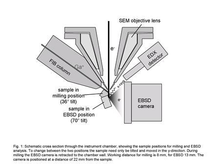
The system described here has been developed on a Zeiss-Crossbeam XB 1540 FIB-SEM which consists of a Gemini-type field emission gun electron column and an Orsay Physics ion beam column mounted 54°
from the vertical. For EBSD, a Digiview camera of EDAX-TSL is mounted on a motorised slide that allows the camera to be driven under the computer-control to its operating position in the chamber and
withdrawn as needed. An energy dispersive X-ray spectroscopy (EDX) detector is mounted such that EBSD and EDX signal can be simultaneously detected. The geometric arrangement of the system is
schematically shown in figure 1. In our system, in contrast to all other already available ones, the EBSD camera and EDX detector are mounted opposite the ion column. This has the significant
advantage, that, in order to change from the milling to the EBSD position, the sample need only be moved about two axes which minimises possible alignment errors. Furthermore, this geometry allows a
large flexibility of the measurement configuration. We will return to this further below.
For EBSD, the investigated surface is usually tilted 70° from the horizontal position. As illustrated in figure 1, this requires a sample tilt between grazing incidence ion milling and EBSD of 34°.
Due to angular limitations of the stage currently used and due to the fact that in EBSD position the EBSD camera is positioned very close to the sample (approximately 20 mm), the sample must be
mounted on a relatively high pre-tilted stage. Therefore, the sampled area cannot be brought into the eucentric tilt position of the stage. Consequently each sample tilt must be combined with a
y-movement of the stage.
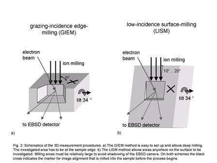
Two 3D-measurement strategies are possible. The first, we term the grazing-incidence edge milling (GIEM) method, illustrated in figure 2a. The sample is prepared by grinding and polishing to produce
a sharp rectangular edge. Milling is then performed under grazing incidence to one surface at this sample edge. After milling has created a smooth surface at the desired distance to the sample
surface, the sample is moved into EBSD position by a 34° tilt and the appropriate y-movement of the stage. EBSD is performed on this surface. After EBSD has completed, the sample is returned to the
milling position and the next cut performed. The method has the advantage of being easy to set-up and allowing investigation of large volumes. In contrast, the microstructure to be investigated must
be close to the edge which is not always easily achieved or possible at all. In this case a second, alternative method may be applied, the low-incidence surface milling (LISM) method, which is
illustrated in figure 2b: The initial sample preparation must produce a fine polished surface. For milling on the free surface the sample is tilted such that the ion beam enters the surface at an
angle of 10 to 20°. As in the GIEM method, the sample is subsequently tilted by 34° and EBSD performed on the milled surface. The advantage of this method is that virtually any volume close to the
sample surface can be investigated. The disadvantage is that the milling area needs to be significantly larger than in the case of GIEM in order to avoid shadowing of the EBSD screen.
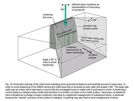
The size and shape of the milled area is determined, on the one hand, by the size of the investigated surface. On the other hand, it has to be considered that the edge of the milled area projects a
shadow onto the EBSD camera. The shadow increases with increasing distance of the milled area from the free sample surface and decreasing distance between the EBSD camera to the surface. For
high-speed EBSD, a large acceptance angle of the diffraction pattern is beneficial. At a camera position of 20 mm we obtain an acceptance angle of approximately 120°. This means that the milled area
must be bound by at least 60° angles on all three edges in order to allow shadow-free diffraction patterns (see figure 17). This additionally milled volume may significantly increase milling time at
large milling depths or when applying the LISM method. A reasonable alternative is to remove the shadowing areas with a large ion beam current and mill only the investigated surface with a small and
therefore finely focused ion current. This is accomplished in our system by setting-up a milling list which holds a number of user-defined milling areas.
For both measurement strategies, a position marker is required that allows accurate positioning of the sample after movement from EBSD observation to milling or vice versa. As a position marker we
use a cross that is milled next to the measured area into the sample surface. A single marker is sufficient since only translations are needed (no sample rotation is applied). The accuracy of sample
positioning will be discussed further in section 4.
2.2 Automatic 3D orientation microscopy
Running the 3D milling and EBSD cycle fully automatically requires a number of instruments and processes to be synchronised: for orientation microscopy the SEM, the EBSD program, the camera slide
controller, the camera controller and the electron image drift correction program need to cooperate. For sectioning, the FIB and the FIB image drift correction program are required. Finally for
changing between milling and EBSD position the sample stage needs to be accurately controlled. All participating processes are controlled by one 3D measurement program. Once the software is
configured, it runs the milling and EBSD cycle until a predefined number of cycles has been reached.
A cycle consists of the following steps:
(i) The EBSD camera is moved into position in the chamber.
(ii) The position marker is detected by image cross-correlation and the sample brought to its reference position using beam shift functions.
(iii) A reference image is taken in EBSD position.
(iv) Orientation mapping is performed using the predefined camera control parameters.
(v) After orientation mapping has been fully accomplished the camera is retracted, the stage is moved to the predefined milling position and the FIB gun is switched on if it was
off.
(vi) The microscope is switched to FIB mode and the position marker is detected by cross correlation. A shift of the FIB beam brings the milling area into reference position.
(vii) A reference image is taken using the FIB beam to document the milling progress from the FIB position.
(viii) The FIB switches to milling mode, steps the beam forward to the desired z-step size, and performs the milling list.
(ix) Once milling is finished the FIB-gun is switched off, if requested, and the stage is moved back to the predefined EBSD position.
Automatic 3D orientation microscopy puts high demands on the measurement process: (1) the stage positioning has to be accurate enough to allow redetection of the marker in each position in the limits of the beam shift controls. (2) The precision of stage tilt must be high enough to avoid any visible distortion of the field of view. (3) Stage drift after sample repositioning must be minimized and the stage must reliably come to a complete stop in the range of tens of seconds. (4) The position correction algorithm must be precise enough to achieve the desired resolution. (5) The SEM and the FIB must work stably over long measurement times. All of these demands are fulfilled on the here presented system. We discuss the limits further in section 4.
2.3 Software for 3-dimensional data analysis
For the analysis of 3D data, so far rudimentary software has been developed. It allows viewing any position in space of the measured volume by sequential display of 2D-microstructure images. Using the mouse any position in the measured volume can be selected and zoomed out or in. Additionally movies on the 3D stacking can be shown for any position. This allows understanding of the 3D microstructure. For preparation of the individual slice images the batch processing function of the EDAX-TSL OIM Analysis software package is used. This function allows applying similar operations to any number of measured data sets, for example rotation of the reference system, clean-up, map construction and saving of images to disk.
The 3D software furthermore contains a tool that allows manual selection of grain boundaries or other interfaces. Subsequently the local grain boundary
normals in the sample and crystal reference systems are calculated. It therefore enables access to data which can only be gained by 3D analysis.
An important precondition for clear rendering of 3D data is the precise alignment of the slices. Although this is achieved to a large extent during the data acquisition process the data still show
misalignment between the slices. We therefore developed an alignment tool which is based on the calculation of a correlation function was quantifies the values of the 3 Euler angles at a position x,y
in the template orientation map that are subtracted one by one from those at the position x+i, y+j in the working map. The position where the sum of all differences Cij is at a minimum produces the
best alignment. Note, that before Cij is calculated the Euler angles must be reduced to a single symmetric variant.
Other groups have developed more advanced software. A well-known software package for 3D rendering is, for example, the program IMOD that is based on the construction of 3D wire-frame models from 2D
cuts [27]. We have used the software ourselves for the presentation of 3D data [9], however, a serious disadvantage is the enormous manual work required for model preparation. Others have developed
software that allows the selection of 3D grains and the determination of volume properties of these grains, e.g. [22]. A very powerful 3D representation of grain boundaries has been presented by
Rowenhorst et al [28], who use a colouring of grain boundaries according to the position of its local crystallographic normal vector in a standard orientation triangle.
3 Application examples
In this section, four selected examples on 3D materials analysis are presented measured using the described system. The selection of the samples has been made such that the strengths and the limits
of the system can be well demonstrated. The strengths lie clearly in the spatial resolution, in the precise definition of microstructure which allows, for example, deformed or multiphase material to
be characterised, and in the ease of operation. The limits are confined by the relatively small investigable volume and by possible material/microstructure alteration due to ion beam
irradiation.
For all measurements presented, the ion beam column was operated at an accelerating voltage of 30 kV with beam currents between 100 pA and 2 nA . For EBSD, an electron accelerating voltage of 15 kV
was used. The EBSD camera was always positioned approximately 20 mm away from the sample. All EBSD measurements were performed at a high measurement rate of 65 to 70 patterns per second. This could
only be accomplished by minimizing pattern indexing calculation time. To this end, in multiphase materials only the most simple phase was indexed on-line. The complete indexing for all phases was
then performed off-line from the recorded Hough-peak data using the full crystallographic information.
3.1 Pearlite
Pearlite is a lamellar arrangement of ferrite (-Fe with bcc lattice structure) and cementite (Fe3C) that forms in a eutectoid reaction from austenite (-Fe with fcc lattice structure). In
two-dimensional investigations, pearlite often exhibits characteristic bending of the lamella structure which is related to a significant orientation change of the ferrite and likely also of the
cementite. The latter information is not quite certain because the crystal orientation of cementite is very difficult to measure by electron diffraction techniques due to its low structure factors.
The occurrence of bending and of the related orientation change is an interesting hint on the physical mechanism of phase transformation. A number of models have been proposed to explain the pearlite
formation, e.g. [29][30][31]. A 3D investigation of the arrangement of pearlite lamellae yields new and otherwise inaccessible information : first, the direction of maximum orientation gradients may
be determined and spatially correlated with the strength of lamella curvature. Second, the ferrite-cementite phase boundary might be precisely characterised with respect to the ferrite grain boundary
normal.
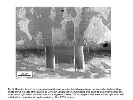
For our 3D investigations a simple high carbon steel Fe 0.49% C sample has been selected. The sample was heated to 950°C and then furnace cooled at a rate of 0.1°C/s. Figure 3a shows the remaining
microstructure of the pearlite colonies after milling. The cementite lamella (white) had a width of 100 to 200 nm and a distance varying between 200 and 400 nm. The measurement system has been set-up
for a GIEM measurement. 50 slices of 30 x 20 µm² were milled with a step size of 100 nm. Orientation mapping was performed using as well a lateral step size of 100 nm. Only the ferrite phase was
indexed since cementite did not produce any indexable patterns. The time for one complete cycle was approximately 35 minutes including 16 minutes for milling and 15 minutes for EBSD
mapping.
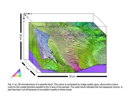
Figure 4 displays the result of the measurement in the form of a 3D orientation map where the colour of each voxel (volume pixel) is a combination of the diffraction pattern quality which defines the
brightness of the voxel and the orientation of the measurement plane normal which defines the colour according to the inverse pole figure colour triangle. Though cementite could not be indexed, the
reduced diffraction pattern quality indicates the position of the lamellae . The figure shows the high alignment accuracy of the measurement: at many positions, it is possible to track the pearlite
lamella through all three dimensions. Nevertheless, in areas where the lamellae are close together their exact direction is not clear. We discuss problems of alignment in section 4. The strong
orientation change across the volume is displayed in figure 5a, where the colour code denotes the misorientation angle of a given voxel with respect to a reference orientation. As reference, the
orientation of the lamella-free area in the upper back corner is selected. The maximum indicated misorientation is 15°.
Figures 4 shows that the observed pearlite consists of 2 grains. It is interesting to see that the strong continuous orientation gradients run parallel to the pearlite lamellae. Generally, no
continuous orientation change occurs perpendicular to the lamellae; however, small angle grain boundaries are found to lie mainly parallel to the lamellae. The convergence of the orientation gradient
with the lamella position shows that the orientation gradient is directly related to the growth process of the lamellae.
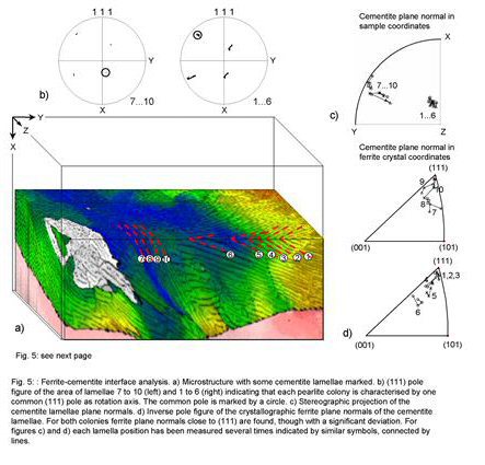
One of the most significant advances of 3D orientation microscopy compared to the 2D technique is the opportunity to determine grain or phase boundary planes. Currently a semi-automatic tool is
applied to measure the position of boundary planes. From 3 user-defined points on a plane the plane normal vector with respect to the sample and crystal coordinate system is calculated. The results
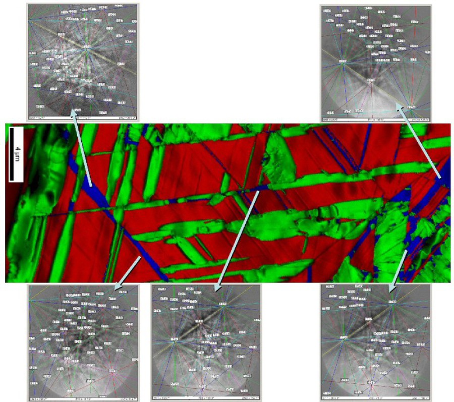
are demonstrated in figure 5. Two sets of pearlite lamellae, 1 to 6 and 7 to 10 have been investigated. As indicated by the pole figures in fig. 5b, in each of the lamellae groups the ferrite
crystals continuously rotate about a (111) plane. The rotation pole, however, is different for both groups. The position of the lamellae normals relative to the sample reference frame is displayed in
the pole figure in fig. 5c. The crystallographic indices of the ferrite side of the lamellae boundaries are shown in the inverse pole figures in fig. 5d. The inverse pole figures show that the
ferrite phase boundary is close to (111); albeit, with a significant deviation of up to 16°. This deviation is due, only to a minor part, to measurement inaccuracies, i.e. inaccuracies in spatial
measurement and orientation determination. It has been shown by TEM investigations that the atomic habit plane of ferrite-cementite lamellae may be ( 1 2 5), (1 1 2) or (0 1 1) (see [32], [33], for
example), depending on the orientation relationship between both phases. While the (111) plane determined here deviates considerably from these results, it has, in fact, been shown that there is not
necessarily any correspondence between the atomic habit plane and the macroscopic one [34]. Furthermore, from the present results it seems that there is also no clear relationship between crystal
orientation and macroscopic habit plane.
3.2 "Nanocrystalline" NiCo deposits
Electrodeposition from aqueous solution has been intensively studied as a method to create metallic films with nanocrystalline microstructure [35][36][37][38][39][40] The deposition parameters, such
as solution composition, current density and bath movement strongly influence the developing microstructure. The exact mechanisms of microstructure formation are still largely unknown, also because a
precise characterisation of the microstructure has rarely been undertaken. In a recently published work [41] we applied EBSD-based high resolution orientation mapping to obtain a deeper knowledge on
the microstructure of electrodeposited thin films of NiCo. Most of the investigated films consist to a large volume fraction of columnar crystals with cross sections in the sub-micrometer range but
lengths in the order of more than 30 µm. For all columnar grains the direction is close to the growth direction of the crystal column. Only in niches besides these crystals do areas of truly
nanocrystalline material exist. We found furthermore that the elongated crystals are in most cases growing in triples of 3 parallel crystals which are related to each other by a twin orientation
relationship. The existence of these triples can be seen on the free grown surface of the electrodeposited material in the form of 3-fold pyramids. We suspect that the existence of twins stabilizes
the growth of columnar grains by formation of low energy boundaries. Thus, twin formation probably prevents the formation of truly nanocrystalline volumes.
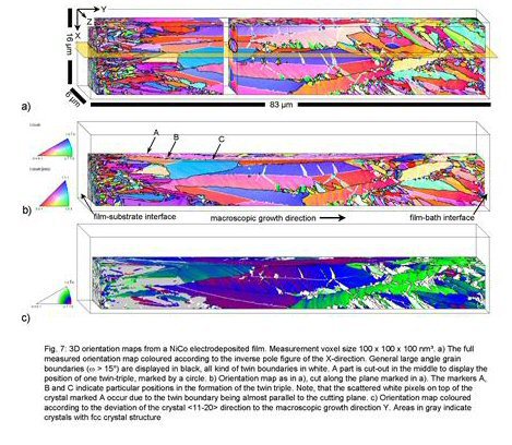
3D orientation microscopy was performed on a full, 100 µm wide cross section of an electrodeposited material. The sample was manually grinded and polished on the cross sections to produce a sharp
rectangular edge. The sample before milling is shown in figure 6. 3D orientation microscopy was performed using the GIEM method. A step size of 100 nm in all dimensions was selected and 60 maps
covering a volume of 83 x 16 x 6 µm³ were measured within less then 2 days. The results are shown in figure 7a in form of a material block, coloured according to the inverse pole figure of a
direction perpendicular to the growth direction. Usual large angle grain boundaries are coloured black while all possible twin boundaries are displayed as white lines. In the centre of the block a
part has been cut out to display a typical twin-triple. In figure 7b the block is cut along the plane that contains the twin triple indicated in 7a. The triple is not growing straight but is visibly
quite heavily curved. Together with this curvature the orientation of the triple changes as shown in figure 7c which displays the deviation of the macroscopic growth direction from the crystal
direction. The crystal orientation is continuously deflected by the regular occurrence of some sort of lattice defects. The nature of these lattice defects, visible in form of inclined stripes in
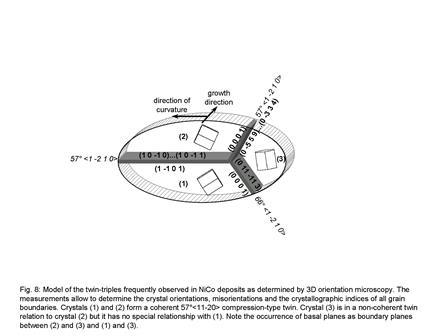
figure 7c, is not yet clear. In the centre of the measured block the twin triple consists of 3 grains with two 56° compression twin relations between them and an approximately 66°
relationship on the remaining boundary (figure 8). From our earlier 2-dimensional investigations [41] we proposed the following formation mechanism for the triple. A primary crystal (1) twins
independently with the same twin relationship into two twin variants (2) and (3) such that all three crystals show a direction parallel to the macroscopic growth direction optimum for quick
growth. The boundary between the crystals (2) and (3) is then automatically fixed to a 66° relationship. In the light of the new 3D data this explanation no longer seems totally correct.
Following the triple in growth direction we first notice that the grains (1) and (2) exist as twins with a sharp 57° relation already when they first enter into the measurement area (marked as
point A in figure 7b) (note that grain (2) is not visible in the figure as it is on top of grain (1)). At point B, grain (3) occurs and grows for the first approximately 10 µm as a very thin tube
parallel to grains (1) and (2). At the position where the grains reach a position for optimum growth (i.e. parallel to the macroscopic GD) grain (3) also expands and grows larger (point C). At
this position we applied the 3D analysis program to determine the grain boundary characteristics. The results are displayed in figure 8: between grain (1) and (2) we find the twin boundary,
typical for these twins [42]. Grain (3), although it shows a precise twin orientation relation with grain (2), does not have a twin boundary with the latter, i.e. the plane indices on both sides of
the grain boundary are different, the one of grain (2) being very precisely the (0001) basal plane, the other one being some quite highly indexed one. The same is true for the boundary with grain (1)
although this grain boundary even does not show any typical twin orientation relationship. We conclude that grain (3) is a twin of grain (2) but its boundary is incoherent and therefore of a quite
different quality than that between (1) and (2). It seems furthermore that the (0001) basal plane forms a low energy boundary both in case of incoherent twins ((2)-(3)) as well as of conventional
large angle grain boundaries ((1)-(3)).
3.3 Deformation and crystallographic orientation patterns below nano-indents in Cu single crystals
As another example of the application of the new 3D orientation imaging method we conducted a 3D study at sub-micrometer-scale resolution on the microstructure and crystallographic texture below sets
of conical nano-indents which were placed using different forces in a Cu single crystal with (111) indentation plane normal. The motivation for this investigation is to understand the formation of
complex crystallographic orientation patterns below indents.
In a set of recent papers the group of Larson et al. [43][44][45][46] presented results on the microstructure evolution below micro-indents by using a non-destructive 3D synchrotron diffraction
method. In their work, the authors observed a systematic deformation-induced orientation pattern below indents in Cu single crystals with (111) indentation plane normal. The experimentally observed
patterns were characterized by outward rotations at the rim of the indent (tangent zone of the indent) and inward rotations directly below the indent close to the indenter axis. The results were
discussed in terms of Kröner’s concept of geometrically necessary dislocations. Zaafarani et al. [26] investigated orientation patterns below nano-indents in (111) Cu crystals using a manual 3D EBSD
method. These experiments revealed a pronounced deformation-induced 3D lattice rotation field below the indent. In the (112) cross section planes below the indenter tip the observed
deformation-induced rotation pattern was characterized by an outer tangent zone with large absolute values of the rotations and an inner zone closer to the indenter axis with small rotations. Further
similar studies on the microstructure evolution below small-scale indents were published also by other authors [47][48][49].
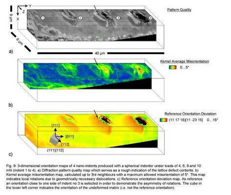
In this work, we report on a more systematic study along these lines. The conical nano-indents wereplaced into a (111) Cu single crystal using different forces, namely, 4, 6, 8, and 10 mN.
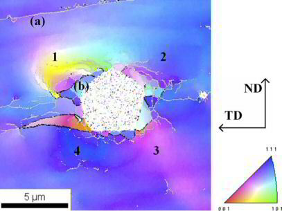
Fig. 9 shows a 3D view of the volume around the 4 different (111) indents. A sequence of sections for the 3D orientation maps were taken perpendicular to the indenter axis. Fig. 9a shows the EBSD
pattern quality in the vicinity of the indents in terms of a gray scale. The pattern quality is a general measure for the local defect density. Fig. 9b shows the kernel average misorientation as a
measure for strongly localized orientation gradients, also indicating the density of geometrically necessary dislocations and Fig. 9c reveals the orientation difference relative to a common reference
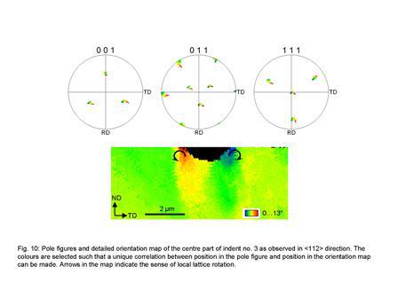
orientation. The latter image, hence, reveals the absolute magnitude of the deformation-induced lattice rotations. Fig. 10 shows, in a more detailed section, the lattice rotations directly under the
indenter axis in a (112) plane perpendicular to the indented (111) plane. This figure shows that the maximum lattice rotation with respect to the original orientation created under the indent is in
the order of 7 to 8°. The sense of the lattice rotation, indicated by arrows, is of opposite sign on the two sides of the indent. The 3D maps in figure 9 gives further interesting insight in the 3D
distribution of the lattice rotation. Following a tangential vector along the dashed circle in fig. 9c, indent 3, the magnitude of the lattice rotation is highest in [011] directions and slowly
fades away while approaching the [112] directions. The sense of rotation remains constant if one follows the tangential vector.
A further interesting result is revealed by comparison of figs. 9a, 9b and 9c: fig. 9a shows the existence of 2 concentric rings of very low pattern quality around the indent (indicated by
arrows in the figure) (note that this feature is actually a ring rather than a shell). This area corresponds to an area of high kernel average misorientation values in fig. 9b indicating a high
density of geometrically necessary dislocations (GNDs). These lead to very strong orientation changes, visible in fig. 9c as a rapid change of colour. The rings have different diameters depending on
the indentation load. Since all previous investigations of the deformation and texture patterns below indents were not reproduced in full 3D maps like in this study these concentric reorientation
rings were not yet reported in the literature.
Another very important result from the figures is that, although the four indents were taken at different indentation forces, they all show basically very similar rotation patterns. This means that
the characteristic orientation pattern is created already at a very early stage of the indentation process and is not gradually built up at higher forces during loading.
3.4 Fatigue crack in Aluminium
The formation of fatigue cracks is an important problem in aluminium alloys used in high cycle fatigue conditions, e.g. in aircraft construction elements. In order to optimise alloys against fatigue,
the mechanisms of damage have to be well understood, in particular with regard to microstructure and crystallography. Crack formation in the aerospace alloy Al 7075-T651 has been intensively studied
by Weiland et al. [50]. They found that cracks start at particles close to the surface and grow into the bulk material. Since a crack is a 3D feature, 3D orientation microscopy is an ideal tool to
study its microstructure and crystallography. To a certain extent, the strain distribution along the crack path may also be revealed from the small orientation changes created by dislocations emitted
from the crack tip during crack growth. For the observation of cracks nucleated at particles, the GIEM procedure is inadequate because it is, first, difficult to prepare a sample such that an
appropriate crack is positioned close to a sample edge, and, second, cracks developing at edges may behave very different from those developing on the free surface and, finally, cracks at edges are
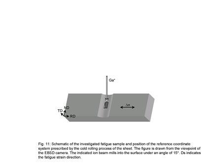
frequently not observed in full. LISM is therefore the ideal method. Figure 11 shows the shape of the investigated sample and the used measurement geometry.
For the present study, 38 slices have been cut and observed at a location near the centre of the trench. The milling area was 34 µm wide and extended over a height of more than 50 µm for the last
slices. Each slice had a thickness of 200 nm, milled at 15° into the surface. Orientation microscopy was carried out with a lateral step size of 200 nm. Summarizing, a volume of 34 x 50 x 7.6 µm³ (x
y z) has been investigated with a 3D step size of 200 x 200 x 200 nm³, .
Figure 12 shows a cracked particle on the surface of the material, recorded with a backscatter detector. The particle has a surface diameter of approximately 10 µm. Figure 13 is a micrograph taken in
EBSD position after 8 cuts with a secondary electron detector. On the very right side a portion of the alignment marker is visible. To the left and right side of the observation area, small strips
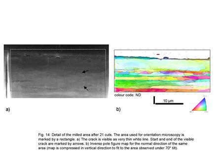
are milled with a large ion current in order to avoid shadowing. The particle is still visible in the image but it is about to disappear. Fig.14 shows the area after 21 cuts: The particle has
completely disappeared, but the crack, visible in (a) as a fine white line, continues into the matrix material. In figure 14b the appropriate orientation map (see below) is shown. It indicates that
the crack extends over several grains as will be discussed further down.
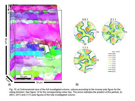
The measured orientations were rotated such that they correspond to the reference system indicated in fig. 11. From the orientation data microstructure maps were created: for the display of crystal
orientations inverse pole figure (IPF) maps for the normal and rolling direction (ND and RD) were selected. The IPF maps are overlaid with a gray value map indicating the diffraction pattern quality.
Figure 15 a shows the RD-IPF map of the entire characterised volume. Due to its narrowness, the crack is difficult to reveal in the orientation maps. Nevertheless, the thin area of lower image
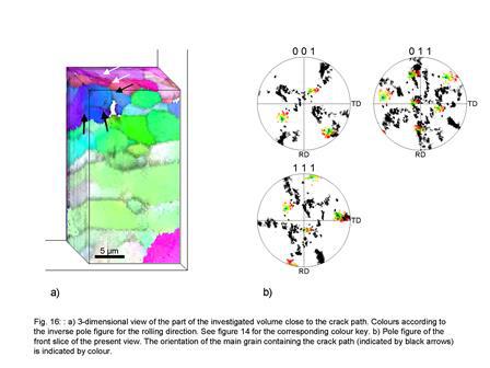
quality, highlighted by the black arrows in the 3D map displayed in figure 16a, corresponds to the position of the crack. It is found that the crack continues below the particle mainly inside of the
grain that also contains the particle. It does not follow any obvious grain or subgrain boundary. The crack extends into a number of differently oriented grains as indicated by white arrows in the
map in figure 16a.
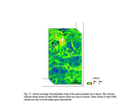
In order to determine local misorientation fields, 2D kernel average misorientation (KAM) maps have been calculated from the orientation data. The KAM is calculated by determining the average of all
misorientation angles between a “ring” of pixels surrounding a kernel of pixels and the pixel at the centre of the kernel. KAM maps indicate the occurrence of local crystal rotations. These, however,
may be created by a regular arrangement of dislocations, for example a dislocation pile-up at (sub)grain boundaries. They, therefore, may be interpreted in terms of local fields of plastic strain as
well. A 3D view of 2D KAM maps is shown in figure 16c. Areas with high KAM values are mainly small angle grain boundaries but also, the crack positions are turning out as areas of higher local
misorientations (partly marked with arrows). This may indicate that crack progression leads to the formation of regular dislocations which remain in the material.


4 Discussion: Accuracy and Application Limits
The above examples have shown that our newly developed 3D orientation microscopy system fully preserves the powerful functions of EBSD-based 2D orientation microscopy and extends them into the 3rd
dimension. At each volume pixel in space, a multi-dimensional vector of data is obtained which includes the crystallographic phase, the crystal orientation and an indication of the lattice defect
density via EBSD pattern quality. If determined also the elemental composition as measured by simultaneous EDS analysis may be included
Important parameters to assess the performance of the system are (i) the spatial resolution, (ii) the angular resolution, (iii) the maximum size of the observable volumes with regard to the long-term
stability of the instrument and (iv) the ability to render artefact-free microstructures. We will discuss each of these parameters separately.
(i) The spatial resolution of the system results from the lateral resolution achieved on the 2D sections, the accuracy of alignment of the sections and the depth resolution. The lateral resolution of
EBSD-based 2D orientation microscopy has been shown to be on the order of few 10nm on a field emission gun (FEG) SEM, depending on the material investigated and the microscope parameters used [18].
Alignment of the serial sections is achieved by application of image recognition software that detects the position of a marker in the image and then applies a beam shift to align this marker with a
previously stored position. Image recognition and alignment is possible with an accuracy of 1 or 2 pixels in the digital image. On the present system, the pixel size on the viewing screen is 0.27 mm
which corresponds to 27 nm at 10000 x on-screen magnification. This value is very close to the lateral resolution of the EBSD technique. At 5000 x magnification a resolution of 50 nm to 100 nm is
achievable. A prerequisite for achieving this resolution is that the alignment marker lies within the visible image after each stage repositioning. The stage must be accurate enough to guarantee
this. On the present system, the stage positioning accuracy is approximately 2 µm in the x and y directions and 1° for the tilt (see point (ii)) which is sufficient.
The depth resolution, i.e. the information depth of EBSD was found to be less than 10 nm [51]. This value, therefore, defines the lower limit of the achievable 3D-depth resolution, as
crystallographic information from slices thinner than 10 nm will overlap significantly. This value is inconsequential as the slice cutting is less precise than this. This is well known from the
preparation of thin foils for TEM via FIB milling where it is difficult to obtain slices thinner than 50 nm. As for the alignment of EBSD slices the accuracy of cutting in the automated system is
defined mainly by the FIB image resolution and the accuracy of automatic image alignment via beam shift. Also for the FIB image, the pattern recognition precision is, at best, as good as one pixel in
the digital image, provided that image resolution is high enough. For a 50 pA beam, which is usually used for image alignment, image resolution is better then 20 nm. Therefore, for a sufficiently
high magnification it is theoretically possible to reach approximately 20 nm depth resolution. In reality we found that the image recognition is usually less precise than 1 pixel, i.e. in the order
of 3 or 4 pixels. Thus, a FIB image magnification of 20000 x is required to reliably obtain 50 nm resolution. We believe that this value represents the highest resolution currently achievable. Most
of the studies performed so far have been carried out with 100 nm step sizes in all directions which gives satisfactory section alignment. It should, however, be noted that not all image alignment
problems have been resolved yet as can be seen in figure 4: the lamella arrangement of pearlite requires a particular precise alignment of the slices, otherwise, due to the narrow spacing, different
lamella may be grouped together by mistake. The continuity of the lamellae is therefore a particularly critical measure for the precision of alignment. There are areas where the lamellae appear
perfectly aligned, particularly on the upper part of the measured block. However, other areas, at the lower part of the milled area in particular, show lamellae which cannot be uniquely grouped
together. The origin of this misalignment is not yet fully clear; but, it is most likely due either to specimen drift during the EBSD measurement or imperfectly flat milled surfaces. In fact, FIB
milling never leads to absolutely flat surfaces; but rather, to slightly curved surfaces which also sometimes show “curtain”-like structures. Figure 17 displays a sketch of a milled surface. A slight
variation in curvature, for example, due to a small variation in sample tilt may lead to a significant misalignment of slices.
(ii) The angular resolution of the classical EBSD technique depends mainly on the size and quality of the recorded EBSD patterns. For high speed measurements it is on the order of 0.5° to 1°. 3D EBSD
may show a larger value due to inaccuracy of the stage tilt. By measuring the orientation variation from slice to slice inside of a well recrystallised grain of constant orientation we found an
average imprecision of tilt of 0.5°. For typical orientation microscopy applications, therefore, the angular resolution of 3D EBSD is as good as that of the 2D technique. Since the angular
misalignment between two slices affects all pixels in a map in a similar way it can be approximately determined – and thus corrected – by calculation of the average misorientation of all neighbouring
points in neighbouring slices excluding all points that have a misorientation larger than a certain threshold value.
(iii) The maximum size of the observable volume depends mainly on the material and on the time investment one wants to make. While the width of the milled surface is virtually unlimited, the height
of the observable surface depends on the sensitivity of the material to curtaining. As indicated in figure 17, from a certain distance to the top edge of the milled area, intense curtaining prevents
the formation of good EBSD patterns and renders the depth position very imprecise. The distance where curtaining starts depends strongly on the material, its microstructure and crystal orientation,
the quality of the top surface and the milling current. To date, the largest curtain-free height obtained is 30 µm on a large-grained Fe3%Si alloy milled with 500 pA beam current. In principle, as
with the width, the depth of milling is unlimited. However, the further one cuts into a sample the wider the milled volume has to be in order to prevent shadows on the EBSD screen and serious
re-deposition of milled material on the sides of the milled volume. The volume limiting parameter is therefore the milling time: a curtain-free area of 20 x 20 µm may be milled 1µm into a low-alloyed
steel sample in approximately 15 min with a beam current of 500 pA. The sides of the volume may be milled with a larger beam current at a higher rate since they don’t require any surface quality. We
believe that the largest volume investigable in the here presented way is in the order of w x h x d = 50 x 50 x 50 µm³. Other groups have shown that using particular sample preparation (e.g. a
“finger”, prepared by mechanical machining) still larger volumes can be obtained [23].
Large volumes or high resolution measurements require long measurement times and therefore long term stability of the instrument, in particular of the FIB gun . On the Zeiss XB 1540 the stability of
the FIB gun is high enough to perform even measurements lasting as long as 10 days if the FIB gun is switched off during the EBSD measurement. After switching the FIB gun on usually only minutes are
required to obtain stable emission behaviour. The stability of the gun is controlled by the automatic 3D software and milling is performed only after a stable emission current has been
obtained.
(iv) On many metals and intermetallics investigated so far (various steels, nickel, copper, aluminium, FeAl, CuZnAl) excellent diffraction patterns were obtained from milled surfaces and the
microstructures observed on these were similar to those prepared by other methods. Nevertheless, various problems exist. One is the amorphisation of certain materials. We have observed that
Nb-containing Laves-phase inclusions in Fe3Al, which give clear diffraction patterns after mechanical preparation, do not give any patterns when prepared by milling [9]. It is known from silicon,
that Ga+ ion beam milling with 30 kV ions creates an amorphous layer of approximately 20 nm thickness [52] which is too thick for EBSD. On TEM sample preparation low-kV ion polishing subsequently
reduces the thickness of the amorphous layer significantly. It is possible, but not yet tested, that this would help also with 3D orientation microscopy. A second, serious problem has been observed
when milling steels with metastable residual austenite, for example low-alloyed TRIP steels. Here, all austenite transforms under influence of the ion beam into ferrite. Up to now, this
transformation could not be avoided neither by small beam currents nor by low-kV milling. Finally, we have observed that the microstructure of heavily deformed aluminium may be destroyed by intense
ion beam irradiation which can probably be attributed to the formation of a low-temperature melting eutectic.
5 Conclusions
A system for 3D orientation microscopy based on fully automated serial sectioning and EBSD-based orientation microscopy has been developed in a FIB-SEM. The technique yields a multidimensional data
vector for each voxel of the measured volume, including the crystal orientation, the crystallographic phase, a value for the lattice defect density, and, if measured by simultaneous EDS analysis, the
elemental composition. Two milling strategies have been devised which allow 3D microstructures close to the edge of a sample or anywhere on a free surface to be investigated. A volume pixel
resolution of 100 x 100 x 100 nm³ has been obtained as a standard but 50 x 50 x 50 nm³ seems to be realistic optimum. The largest volumes observable are in the order of 50 x 50 x 50 µm³. The
technique works on a large number of materials but some exceptions have been found. In particular, metastable austenite occurring in various steels seems not to be accessible by the technique because
it transforms into ferrite under Ga+-ion beam irradiation.
The functionality of the system has been demonstrated by means of a number of high resolution 3D microstructure studies. The structure of pearlite lamellae with a distance of 100 to 200 nm has been
studied. At most locations an accurate structure reconstruction is obtained. The 3D orientation gradients follow a direction parallel to the lamellae. Using a manual procedure, the macroscopic habit
planes of some of the lamellae were indexed. It was found that these planes do not correspond to the atomic habit planes determined by transmission electron microscopy. In a second study, the 3D
microstructure of an electrodeposited thin film of NiCo was investigated. It was shown that the system is able to resolve small grains with a grain size in the order of 300 nm and that it is an
excellent tool to fully characterise the complex twin structures frequently occurring in this material. Third, a study on the 3D deformation pattern created by nanoindentation in a Cu single crystal
was conducted. It was found that indentation creates concentric rings of strong lattice rotation about the indenter axis. Along these rings the intensity of rotation changes in a regular manner but
the sense of rotation remains constant. The rings occur already at the smallest indentation depth and expand during further loading. Finally, a fatigue crack in aluminium was characterised in terms
of its 3D morphology and crystallography. The crack starts in a particle at the surface and extends through various grains into the material. We suppose that the slight orientation change that is
found along the crack path indicates the emission of dislocations from the crack tip during crack growth.
In comparison to the newly developed 3D x-ray diffraction techniques the 3D orientation microscopy technique has the advantage of a significantly higher spatial resolution, applicability also to
highly deformed or multi-phase structures, and ease of application. A serious disadvantage is the fact that the technique is destructive, that means that once a volume has been investigated, it is
destroyed; thereby rendering in-situ 3D studies impossible. The two techniques appear largely complementary rather than being in direct competition.
6 Acknowledgements
The authors would like to express their thanks to the people of the Zeiss hardware and software development groups, in particular to P. Hoffrogge and P. Gnauck and D. Hubbart and H. Walaart for their
support in building-up the 3D system. Furthermore the authors are grateful to H. Weiland, Alcoa, for initiating the investigations on crack formation and delivering the appropriate sample. The
authors thank T. Takahashi for the preparation of the pearlite sample and N. Zaafarani (MPIE) for the preparation of the nanoindents. Finally the authors would like to thank J. Konrad, A. Bastos and
M. Nellessen, co-workers at the MPIE as well as P. Scutts, D. Dingley and other co-workers at EDAX-TSL, for their help in developing the 3D system.
7 References
[1] B.L. Adams, Met. Trans. 17A, (1986) 2199
[2] B.L. Adams, P.R. Morris, T.T. Wang, K.S. Willden, S.I. Wright, Acta Met 35 (1987) 2935
[3] H.F. Poulsen et al., J. Appl. Cryst. 34 (2001) 751
[4] B.C. Larson et al., Nature 415 (2002) 887
[5] W. Yang et al., Micron 35 (2004) 431
[6] A. Preusser, H. Klein, H.J. Bunge, Solid State Phenomena 105 (2005) 3
[7] E.M. Lauridsen, S. Schmidt, S.F. Nielsen, L. Margulies, H. F. Poulsen, D. Juul-Jensen, Scripta Mat. 55 (2006) 51–56
[8] L. Margulies, G. Winther, H.F. Poulsen, Science 291 (2001) 2392
[9] J. Konrad, S. Zaefferer, D. Raabe, Acta Mat. 54 (2006) 1369
[10] S.V. Prasad, J.R. Michael, T.R. Christenson. Scripta Mat. 48 (2003) 255.
[11] J.R. Michael, J. Schischka, F. Altmann, in: HKL Technology EBSD Application Catalogue 2003, HKL Technology, Hobro, Denmark
[12] T.L. Matteson, S.W. Schwartz, E.C. Houge, B.W. Kempshall, L.A. Gianuzzi, J. Electronic Mater. 31, 2002, 33 - 39
[13] T.T. Sheng, G.P. Goh, C.H. Tung, L.F. Wang, J. Vac. Sci. Tech. B 15 (1997) 610
[14] T.L. Matteson, S.W. Schwarz, E.C. Houge, B.W. Kempshall, L.A. Giannuzzi. J. Electron Mat. 31 (2002) 33.
[15] Z. Cheng , T. Sakamoto, M. Takahashi, Y. Kuramoto, M. Owari, Y. Nihei, J. Vac. Sci. Technol. B 16 (1998) 2473
[16] H. Jin, P.D. Wu, M.D. Ball and D.J. Lloyd, Mater. Sci. Technol., 21 (2005) 419
[17] A. J. Schwartz, M. Kumar, B. L. Adams (eds.), Electron Backscatter Diffraction in Material Science. Kluwer Acad./Plenum Publ., New York 2000
[18] F.J. Humphreys, J. Mat. Sci. 36 (2001) 3833
[19] D. J. Dingley, J. Microscopy 213 (2004) 214
[20] G. Spanos, Scripta Mat. 55 (2006) 3, Viewpoint set no. 41 “3D Characterization and Analysis of Materials”
[21] M.D. Uchic, M. Groeber, R. Wheeler IV, F. Scheltens, D.M. Dimiduk. Microsc. Microanal. 10 (2004) 1136
[22] J.J.L. Mulders, A.P. Day, Mat. Sci. Forum, 495-497 (2005) 237
[23] M.D. Uchic, M.A. Groeber, D.M. Dimiduk and J.P. Simmons, Scripta Mat. 55 (2006) 23
[24] M.A. Groeber, B.K. Haley, M.D. Uchic, D.M. Dimiduk, S. Gosh, Mat. Character. 57 (2006) 259
[25] S. Zaefferer., J. Konrad, D. Raabe, (2005), Microscopy Conference 2005, Davos, 63
[26] N. Zaafarani, D. Raabe, R.N. Singh, F. Roters, S. Zaefferer, Acta Mat. 54 (2006) 1863
[27] J.R. Kremer, D.N. Mastronarde, J.R. McIntosh, J Struct Biol. 116 (1996) 71.
[28] D.J. Rowenhorst, A. Gupta C.R. Feng and G. Spanos, Scripta Mat. 55 (2006) 11
[29] F.A. Khalid and D.V.Edmonds Acta Mat. 41 (1993) 3421
[30] M. Durrand-Charre, Microstructures of steels and cast irons, Springer, (2004)
[31] G.J. Shiflet, Mater. Sci. Eng., 81 (1986) 61
[32] D.S. Zhou, G.J. Shiflet, Met Trans 23A (1992) 1259
[33] G. Spanos, H.I. Aaronson, Acta Metall. Mater. 38 (1990) 2721
[34] S.A.Hackney, G.J. Shiflet, Scripta Metall. 20 (1986) 389
[35] A.Vicenzo, P.L. Cavallotti, Electrochimica Acta 49 (2004) 4079
[36] D. Golodnitsky, Yu. Rosenberg, A. Ulus, Electrochimica Acta 47 (2002) 2707
[37] E.Gómez, J. Ramirez, E. Vallés, J. Appl. Electrochem. 28 (1998) 71
[38] K. Daheum, D.-Y. Park, B.Y. Yoo, P.T.A. Sumodjo, N.V. Myung, Electrochimica Acta (2003) 819
[39] A.M. El-Sherik, U. Erb, J. Mater. Sci. 30 (1995) 5743
[40] B.Y.C.Wu, P.J.Ferreira, C.A. Schuh, Met. Mater. Trans. A, Vol.36A (2005) 1927.
[41] A. Bastos, S. Zaefferer, D. Raabe, C. Schuh, Acta Mater. 54 (2006) 2451
[42] P. G. Patridge, Met. Rev. 12 (1967) 169
[43] W. Yang, B.C. Larson, G.M. Pharr, G.E. Ice, J.Z. Tischler, MRS Symposium Proceedings (2003) 779, W5.34.1
[44] B.C. Larson, W. Yang, G.E. Ice, J.D. Budai, J.Z. Tischler, Nature 415 (2002) 887
[45] R.I. Barabash, G.E. Ice, B.C. Larson, G.M. Pharr, K.S. Chung, W. Yang, Appl. Phys. Lett. 79 (2001) 749
[46] G.E. Ice, B.C. Larson, Adv. Eng. Mater. 2 (2000) 643
[47] Y. Liu, B. Wang, M. Yoshino, S. Roy, H. Lu and R. Komandri, J. Mech. Phys.Solids 53 (2005) 2718
[48] K.K.McLaughlin, N.A. Stelmashenko, S. J. Lloyd, L.J. Vandeperre and W.J. Clegg, Mater. Res. Soc. Symp. Proc. 841 (2005), 3
[49] D. Kiener, R. Pippan, C. Motz and H. Kreuzer, Acta Mater. 54 (2006) 2801
[50] H. Weiland, S. Cheong, J. Nardiello, S. Zaefferer, J. Papazian, Dierk Raabe, submitted to J. Fatigue
[51] S. Zaefferer, Ultramicroscopy (2006), available on-line since 09/2006
[52] Kato et al., J.Vac. Sci. Tech. A17(1999) 1201
Simplified nondestructive 3D EBSD method that enables measurement of all 5 degrees of freedom of grain boundaries combined with segregation analysis using atom probe tomography.
2014 scripta Mandal GB segregation 3D EB[...]
PDF-Dokument [972.8 KB]
Orientation gradients and geometrically necessary dislocations (GND) in ultrafine grained dual-phase steels studied by 2D and 3D EBSD
Mater_Science_Engin_A 527 (2010) 2738.pd[...]
PDF-Dokument [2.2 MB]

 3D EBSD in Fe3Al: Konrad et al. Acta Mater. 54 (2006) 1369
J. Konrad, S. Zaefferer, D. Raabe
Acta Materialia 54 (2006) 1369-1380
Acta Materialia 54 (2006) 1369–1380 3D E[...]
PDF-Dokument [902.4 KB]
We present a study of the microstructure around a hard Laves particle in a warm-rolled intermetallic Fe3Al-based alloy. The experiments are conducted using a
system for three-dimensional orientation microscopy (3D electron backscattering diffraction, EBSD). The approach is realized by a combination of a focused ion beam
(FIB) unit for serial sectioning with high-resolution field emission scanning electron microscopy with EBSD. We observe the formation of steep 3D orientation
gradients in the Fe3Al matrix around the rigid precipitate
which entail in part particle-stimulated nucleation events in the immediate vicinity of the particle. The orientation gradients assume a characteristic pattern around the
particle in the transverse plane while revealing an elongated tubular morphology in the rolling direction. However, they do not reveal a characteristic common rotation axis. Recovered areas in
the matrix appear both in the transverse and rolling directions around the particle. The work demonstrates that the new 3D EBSD-FIB technique provides a new level
of microstructure information that cannot be achieved by conventional 2D-EBSD analysis.
Acta Materialia 57 (2009) 559–569 size e[...]
PDF-Dokument [1.9 MB]
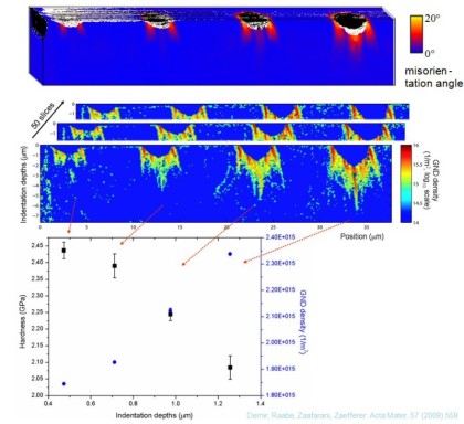 Analysis of indentation size effect by 3D EBSD
Micron 40 (2009) 151 Epsilon martensite.[...]
PDF-Dokument [1.3 MB]
We study the Bauschinger effect on a bent and straightened micro-sized single-crystal copper beam (width: 8.64 um; thickness: 7.05 um) over three consecutive cycles. The reverse yield strengths (straightening step) are much smaller than those in forward loading (bending step). An upper bound estimate shows a load drop of 73% (1st cycle), 76% (2nd cycle) and 83% (3rd cycle) relative to the forward yield stress. Electron backscatter diffraction reveals a dramatic reduction in the bending-induced misorientation gradients upon load reversal (straightening), documenting an unexpected form of microstructure reversibility. The observed Bauschinger softening is interpreted in terms of two effects. The first consists of internal backstresses that support load reversal. They are created by polarized
Acta Materialia 58 (2010) 6055_Bausching[...]
PDF-Dokument [940.0 KB]
J Mechanics Physics Solids vol 58 (2010)[...]
PDF-Dokument [956.1 KB]
Influence of plastic strain, strain rate and cooling rate on the Burgers orientation relationship and variant morphology during beta-alpha phase transformation in a near alpha titanium alloy
Mater-Sc-Engin-A 549 (2012)-Titanium.pdf
PDF-Dokument [2.8 MB]