ECCI (Electron Channeling Contrast Imaging) in the SEM and its application to high Mn steels
Coupling of electron channeling with EBSD: towards the quantitative characterization of deformation structures in the SEM
Abstract
The coupling of electron channeling contrast imaging (ECCI) with EBSD provides an efficient and fast approach to perform ECCI of crystal defects, such as dislocations, cells, and stacking faults, under controlled diffraction conditions with enhanced contrast. From a technical point of view, the ECCI technique complements two of the main electron microscopy techniques, namely, EBSD and TEM. In this review, we provide several application examples of the EBSD-based ECCI approach on microstructure characterization, namely, characterization of single dislocations, measurement of dislocation densities and characterization of dislocation substructures in deformed bulk materials. We make use of a two-beam Bloch wave approach to interpret the channeling contrast associated to crystal defects. The approach captures the main features observed in the experimental contrast associated to stacking faults and dislocations.
Introduction to electron channeling contrast imaging
The characterization of deformation substructures is commonly performed by transmission electron microscopy techniques (TEM). The high spatial and angular resolution of TEM allow the characterization of individual crystal defects such as dislocations, stacking faults and point defects, as well as more complex configurations formed by dislocations and deformation twins [1-3]. However, TEM presents some drawbacks such as sample preparation, where extremely thin samples are needed, and reduced observation area. The common methods for TEM sample preparation, namely, electropolishing, ion milling and focused ion beam (FIB), are time consuming and may even modify the microstructure by introducing point defects (for instance, foil thinning by ion milling [4]) or relaxing internal stresses (bulk thinning prior to electropolishing [5]). Furthermore, the resulting TEM foil offers only a limited observation area (~ 100 × 100 mm2) making it difficult to perform quantitative microstructural characterization required in many topics in materials science. While TEM has proven to be a very versatile tool for the characterization of crystal defects, the limitations outlined above have led to the development of diffraction-based methods such as X-ray diffraction (XRD) [6, 7], synchrotron radiation-based techniques [8-10], and 2D/3D electron backscatter diffraction (EBSD) techniques [11-15]. An alternative electron microscopy technique for characterizing bulk deformed materials is electron channeling contrast imaging (ECCI) [16-18]. ECCI is a scanning electron microscope (SEM) technique that makes use of the strong dependence of the backscatter electron (BSE) signal on the orientation of the crystal lattice planes with respect to the incident electron beam due to the electron channeling mechanism. Interestingly, slight local distortions in the crystal lattice produced by the strain fields associated to dislocations yield a modulation in the BE signal that can be detected by available BSE detectors. Accordingly, crystal defects such as dislocations can be imaged by ECCI in the SEM. According to the dynamical theory of electron diffraction, the optimum diffraction contrast for imaging crystal defects in ECCI is obtained by orienting the crystal exactly into Bragg condition for a selected set of intense diffracting lattice planes [19]. However, since the early observations in 1967 by Coates of Kikuchi-like reflection patterns in the SEM, the so-called electron channeling patterns (ECPs) [20], the impact of ECCI in materials science has been rather limited. This is due to the specific tilting conditions required to image crystal defects in ECCI.
To date, two main ECCI set-ups have been developed, namely, forward-scatter electron (FSE) and backscatter electron (BSE)-based methods. FSE-based approaches make use of high-tilt EBSD-type geometries to enhance the intensity of thermally diffuse (or phonon) scattered electrons. The FS detector records the contrast created by the Kikuchi bands intersecting the detector. This configuration, originally used by Czernuszka et al. [21] to image dislocations in Si and Ni3Ga, has been adapted by Wilkinson’s group [16, 22, 23] and Picard et al. [24-26] to examine dislocations in SiGe/Si epitaxial layers [22], and GaN and SiC thin films [23-26]. BSE-based methods make use of electron channeling patterns to optimize the diffraction contrast of the crystal defect image. These patterns can be obtained after running the microscope at low magnification (so-called electron channeling patterns, ECPs) [17, 18, 20] or after rocking the incoming beam on the material surface by a deflection focusing technique (so-called selected-area channeling patterns, SACPs) [27-29]. The main limitation of these approaches is the large observation area, typically >10 mm, and the low spatial resolution, 2-5 mm. This shortcoming limits the application of ECPs/SACPs-based ECCI set-ups to lightly deformed coarse polycrystals and single crystals [16, 29-32]. Recently, we have proposed the use of EBSD to obtain the rocking parameters of the sample surface under the incoming beam (tilt and rotation angles) where the crystal is oriented into optimum diffraction contrast [33]. Due to the high spatial resolution of EBSD (35±5 nm [34]), crystal defects can be imaged in sub-micrometer areas of deformed bulk materials. In the last few years, we have applied the EBSD-based ECCI approach to several cases, namely, the characterization of complex deformation structures such as dislocation and nano-twin substructures in bulk deformed high-Mn TWIP steels (TWIP: twinning induced plasticity) [35-39], the investigation of dislocation patterns [36, 37, 40], the measurement of dislocation densities in deformed alloys [41, 42] and the characterization of individual dislocations and stacking faults [43, 44]. These studies have demonstrated the feasibility of the EBSD-based ECCI approach on the quantitative characterization of complex deformation structures in bulk materials. From a technical point of view, the ECCI technique complements two of the main electron microscopy techniques, namely, EBSD and conventional diffraction-based TEM. The present paper summarizes the experimental configuration of the EBSD-based ECCI set-up and illustrates its use with several experimental studies. We also provide a physical-based model of ECC contrast associated with crystals defects.
References:
[1] Williams DB, Carter CB. Transmission Electron Microscopy. A Textbook for Materials Science: Springer, 2009.
[2] Thomas G, Goringe MJ. Transmission electron microscopy of materials: John Wiley & Sons, 1979.
[3] Hirsch P, Howie A, Nicholson RB, Pashley DW, Whelan MJ. Electron microscopy of thin crystals. Huntington, NY: Robert E. Krieger, 1977.
[4] Ayache J, Beaunier L, Boumendil J, Ehret G, Laub D. Sample Preparation Handbook for Transmission Electron Microscopy: Springer, 2009.
[5] Mughrabi H. Phil. Mag. 1971;23:869.
[6] Ungár T, Mughrabi H, Wilkens M. Acta Metall. 1982;30:1861.
[7] Ungár T, Ott S, Sanders PG, Borbély A, Weertman JR. Acta Mater. 1998;46:3693.
[8] Jakobsen B, Poulsen HF, Lienert U, Pantleon W. Acta Mater. 2007;55:3421.
[9] Larson BC, Yang W, Ice GE, Budai JD, Tischler JZ. Nature 2002;415:887.
[10] Jakobsen B, Poulsen HF, Lienert U, Almer J, Shastri SD, Sørensen HO, Gundlach C, Pantleon W. Science 2006;312:889.
[11] Wilkinson AJ, Meaden G, Dingley DJ. Ultramicroscopy 2006;106:307.
[12] Pantleon W. Scripta Mater. 2008;58:994.
[13] Zaafarani N, Raabe D, Singh RN, Roters F, Zaefferer S. Acta Mater. 2006;54:1863.
[14] Demir E, Raabe D, Zaafarani N, Zaefferer S. Acta Mater. 2009;57:559.
[15] Field DP, Trivedi PB, Wright SI, Kumar M. Ultramicroscopy 2005;103:33.
[16] Wilkinson AJ, Hirsch PB. Micron 1997;28:279.
[17] Joy DC, Newbury DE, Davidson DL. Rev. Phys. Appl. 1982;53:81.
[18] Schulson EM. J. Mater. Sci. 1977;12:1071.
[19] Spencer JP, Humphreys CJ, Hirsch PB. Phil. Mag 1972;26:193.
[20] Coates DG. Phil. Mag 1967;16:1179.
[21] Czernuszka JT, Long NJ, Boyes ED, Hirsch PB. Phil. Mag. Lett. 1990;62:227.
[22] Wilkinson AJ, Anstis GR, Czernuszka JT, Long NJ, Hirsch PB. Phil. Mag A 1993;68:59.
[23] Trager-Cowan C, Sweeney F, Trimby PW, Day AP, Gholinia A, Schmidt NH, Parbrook PJ, Wilkinson AJ, Watson IM. Phys. Rev. B 2007;75:085301.
[24] Picard YN, Twigg ME, Caldwell JD, C.R. Eddy J, Neudeck PG, Trunek AJ, Powell JA. Appl. Phys. Lett. 2007;90:234101.
[25] Picard YN, Twigg ME. J. Appl. Phys. 2008;104:124906.
[26] Picard YN, Twigg ME, Caldwell JD, Jr. CRE, Mastro MA, Holm RT. Scripta Mater. 2009;61:773.
[27] Essen Cv, Schulson EM, Donaghay RH. J. Mater. Sci. 1971;6:213.
[28] Essen CGv, Schulson EM, Donaghay RH. Nature 1970;225:847.
[29] Morin P, Pitaval M, Besnard D, Fontaine G. Phil. Mag A 1979;40:511.
[30] Pitaval M, Morin P, Baudry J, Viaria E, Fontaine G. Scan. Electron. Microsc. 1977;1:439.
[31] Crimp MA. Microscopy Research Technique 2006;69:374.
[32] Crimp MA, Simkin BA, Ng BC. Phil. Mag. Lett. 2001;81:833.
[33] Gutierrez-Urrutia I, Zaefferer S, Raabe D. Scripta Mater. 2009;61:737.
[34] Zaefferer S. Ultramicroscopy 2007;107:254.
[35] Gutierrez-Urrutia I, Raabe D. Acta Mater. 2011;59:6449.
[36] Gutierrez-Urrutia I, Raabe D. Mater. Sci. For. 2012;702-703:523.
[37] Gutierrez-Urrutia I, Raabe D. Acta Mater. 2012;60:5791.
[38] Gutierrez-Urrutia I, Raabe D. Scripta Mater. 2013;68:343.
[39] Steinmetz DR, Jäpel T, Wietbrock B, Eisenlohr P, Gutierrez-Urrutia I, Saeed-Akbari A, Hickel T, Roters F, Raabe D. Acta Mater. 2013;61:494.
[40] Gutierrez-Urrutia I, Raabe D. Scripta Mater. 2013;69:53.
[41] Eisenlohr A, Gutierrez-Urrutia I, Raabe D. Acta Mater. 2012;60:3994.
[42] Gutierrez-Urrutia I, Raabe D. Scripta Mater. 2012;66:343.
[43] Zaefferer S, Elhami N-N. Submtted to Acta Mater.
[44] Weidner A, Martin S, Klemm V, Martin U, Biermann H. Scripta Mater. 2011;64:513.
[45] Simkin BA, Crimp MA. Ultramicroscopy 1999;77:65.
[46] Zaefferer S. J. Appl. Cryst. 2000;33:10.
[47] Sigle W. Annu. Rev. Mater. Res. 2005;35:239.
[48] Reimer L, Kohl H. Transmission Electron Microscopy. Physics of Image Formation: Springer, 2008.
[49] Joy DC. Monte Carlo Modeling for Electron Microscopy and Microanalysis: Oxford University Press, 1995.
[50] Twigg ME, Picard YN. J. Appl. Phys. 2009;105:093520.
[51] Dudarev SL, Rez P, Whelan MJ. Phys. Rev. B 1995;51:3397.
[52] Winkelmann A, Schroeter B, Richter W. Ultramicroscopy 2003;98:1.
[53] Wilkinson AJ, Hirsch PB. Phil. Mag. A 1995;72:81.
[54] Ham RK. Phil. Mag. 1961;69:1183.
[55] Griffiths D, Riley JN. Acta Metall. 1966;14:755.
[56] Kuhlmann-Wilsdorf D. The LES Theory of Solid Plasticity. In: Nabarro FRN, Duesbery MS, editors. Dislocations in Solids. Volume 11. 2002.
J.-l. Zhang, S. Zaefferer, D. Raabe
Materials Science & Engineering A 636 (2015) 231-242
A study on the geometry of dislocation patterns in the surrounding of nanoindents in a TWIP steel using electron channeling contrast imaging and discrete dislocation dynamics simulations
Materials Science Engin A636 (2015) 231 [...]
PDF-Dokument [1.5 MB]
 J.-l. Zhang, S. Zaefferer, D. Raabe Materials Science & Engineering A 636 (2015) 231-242 A study on the geometry of dislocation patterns in the surrounding of nanoindents in a TWIP steel using electron channeling contrast imaging and dislocation modeling.
Instrumented nanoindentation is an excellent tool for characterising the mechanical properties and the deformation behaviour of materials at nano/micro-scales [1,2]. The mechanical data,
such as hardness and elastic modulus, obtained by nanoindentation are, however, not easily interpretable in terms of macroscopic mechanical properties because of the complex stress and
strain field developed during the test. Although numerous studies were carried out to understand the strain field formed beneath and besides the indenter, a number of questions about
the associated dislocation activities are still unresolved. It is known, for example from 3D EBSD investigations, that fields of different crystallographic rotations are formed below
an indent. Transmission electron microscopy (TEM) observations of nanoindentation provided detailed information of the mechanisms associated with localized deformation. All these
experimental investigations have certain limitations though: The 3D EBSD observations reveal the existence of geometrically necessary dislocations in terms of the detected rotation
patterns but fail to show the actual complete deformation pattern in terms of the underlying dislocations. TEM observations show the true dislocation arrangements but they suffer from
the fact that thin foils have to be used for that and, hence, either lateral or depth directional information cannot be obtained. To a certain extent the missing information can
be complemented by crystal plasticity simulations, as have been carried out in some studies. This approach, however, suffers from adjustable parameters such as latent hardening and
cross hardening parameters, and uncertainties associated with boundary condition treatment such as friction. A significant number of investigations have been reported on
the crystallographic orientation induced patterns around nanoindents
in materials with fcc structure. Most of the works were conducted by comparison of finite element simulations with secondary electron (SE) images or atomic force microscopy
(AFM) profiles. Irrespective of the shape of the indenter used in these studies, four- and two-fold symmetries for {100}- and {110}-oriented crystals were reported. For {111}-oriented
crystals both, six-fold [9] and three-fold [11] symmetries were suggested. In these works the surface topographical pile-up or sink-in patterns were used for comparison between simulation and experimental results. However, detailed information on how these patterns are
actually formed in terms of the underlying dislocation activities was not provided. In addition, the variation of hardness and/or elastic modulus with indentation depth, the so
called indentation size effect, raises a lot of difficulties with obtaining real values of the mechanical properties. In order to understand the size effect numerous studies have been
carried out in investigating the size of the plastic deformation zone as a function of the indentation depth and/or
indenter size. Most of the works were done by numerical calculations or by topographical pile-up or sink-in pattern observations using atomic force microscopy (AFM) and scanning
electron microscopy (SEM). Also, the real lateral extension of the plastic deformation zone was not sufficiently studied in detail yet. In order to overcome some of the mentioned
experimental and
simulation difficulties we used a newly designed technique, referred to as electron channeling contrast imaging under controlled diffraction conditions (cECCI). It allows the direct
observations of crystal defects like dislocations or stacking faults close to the surface of bulk samples. This technique, which has
similarities to dark field TEM, is applied in an SEM and allows probing approximately the first 50–100 nm of material below the surface.
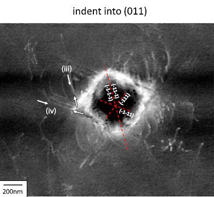
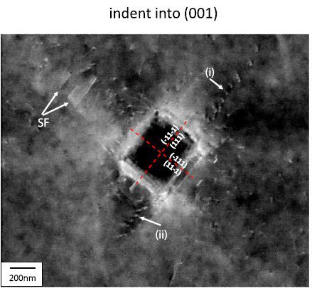
In the present work we applied the cECCI technique to study dislocation structures in the surrounding of nanoindents in a steel with twinning induced plasticity (TWIP) and fcc crystal
structure. Nanoindentation was carried out either in a load-controlled mode with a maximum load or in displacement-controlled mode up to different indentation depths on {100}- {110}-
and {111}-oriented grains in a polycrystalline specimen. The aim of the study is to
understand in more detail the formation of the defects below and next to the indent and to contribute in this way to a better understanding of the pattern formation process. In order to be
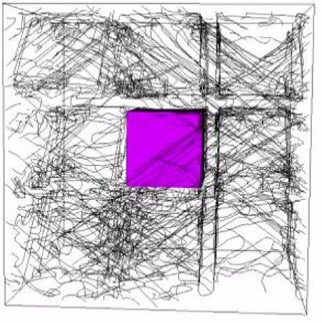
able to interpret our experimental results we also applied discrete dislocation dynamics (DDD) simulations using the Parallel Dislocation Simulator (ParaDiS) code, which shows, to a
certain
extent, which slip systems are active and what the shape and the type of the resulting dislocations in the network is. These data were compared with our experimental results.
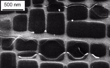
Here, electron channeling contrast imaging under controlled diffraction conditions (cECCI) is used since it enables observation of crystal defects, especially dislocations, stacking faults
and nano-twins, close to the surface of bulk samples. In this work cECCI has been employed to observe defects around nanoindents into the surface of {100}-, {110}-, {111}-oriented grains in
a Fe–22Mn–0.65C (wt%) TWIP steel sample (fcc crystal structure, stacking fault energy 20 mJ/m²) using a cone-spherical indenter. The dislocation patterns
show four- and two-fold symmetries for the {100}- and {110}-orientation, and a three-fold symmetry for the {111}-orientation which is, however, difficult to observe. Discrete dislocation
dynamics (DDD) simulations of the indentation were carried out to complement the static experimental investigations.
The simulations were carried out with both, cross-slip disabled and enabled conditions, where the former were found to match to the experimental results better, as may be expected for an fcc
material with low stacking fault energy. The 3-dimensional geometry of the dislocation patterns of the different
indents was analysed and discussed with respect to pattern formation mechanisms. The force–displacement curves obtained during indentation showed a stronger strain hardening for the
{111} oriented crystal than that for the other orientations. This is in contrast to the behaviour of, for example,
copper and is interpreted to be due to planar slip. Irrespective of orientation and indentation depth the radius of the plastically deformed area was found to be approximately 4 times larger
than that of the indenter contact area.
Acta Materialia 109 (2016) 151-161
On the origin of creep dislocations in a Ni-base, single-crystal superalloy: an ECCI, EBSD, and dislocation dynamics-based study
Ram et al Ni base superalloy creep dislc[...]
PDF-Dokument [2.2 MB]
Nickel-base superalloys are employed in high-temperature applications,
particularly for jet propulsion and power conversion. To increase creep resistance, these alloys are produced as single crystals. Single-crystal superalloys are often fabricated by
directional solidification techniques using competitive dendrite growth.
This work investigates the origin of creep dislocations in a Ni-base, single crystal superalloy subject to creep at an intermediate stress and temperature. Employing high angular resolution
electron backscatter diffraction (HR-EBSD), electron channeling contrast imaging under controlled diffraction conditions
(cECCI) and discrete dislocation dynamics (DDD) modelling, it is shown that low-angle boundaries - which correspond to dendrite boundaries or their residues after annealing - are not the major
sources of creep dislocations. At the onset of creep deformation, they are the only active sources. Creep dislocations are emitted from them and percolate into the dislocation-depleted
crystal. However, the percolation is very slow. As creep deformation proceeds, before the boundary-originated dislocations move further than a few micrometers away from their source
boundary, individual dislocations that are spread throughout the undeformed microstructure become active and emit avalanches of creep dislocations in boundary-free regions, i.e. regions
farther than a few micrometer away from boundaries. Upon their activation, the density of creep dislocations in boundary-free regions soars by two orders of magnitude; and the entire
microstructure becomes deluged with creep dislocations. The total area of boundary-free regions is several times the total area of regions covered by boundary-originated creep
dislocations. Therefore, the main sources of creep dislocations are not low-angle boundaries but individual, isolated dislocations in boundary-free regions.
Acta Materialia 87 (2015) 86--99
Acta Materialia vol 87 (2015) 86 ECCI fa[...]
PDF-Dokument [3.0 MB]
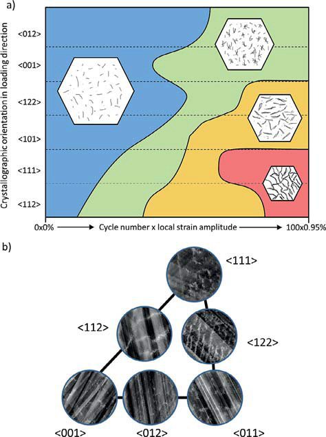
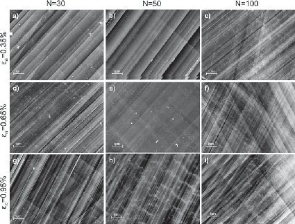
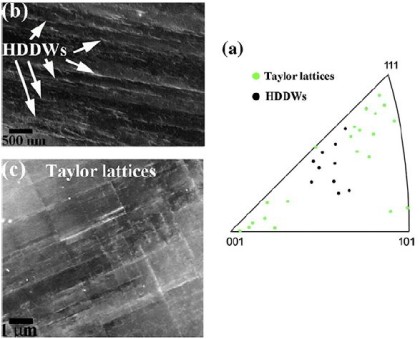
Substructure analysis on cyclically deformed metals is typically performed by time-consuming transmission electron microscopy probing,
thus limiting such studies often to a single parameter. Here, we present a novel approach which consists in combining electron backscatter diffraction
(EBSD), digital image correlation and electron channelling contrast imaging (ECCI), enabling us to systematically probe a large matrix of different
parameters with the aim of correlating and comparing their interdependence. The main focus here is to identify the influence of cycle number, initial
grain orientation and local strain amplitude on the evolving dislocation patterns. Therefore, experiments up to 100 cycles were performed on a polycrystalline
austenitic stainless steel with local strain amplitudes between 0.35% and 0.95%. EBSD and ECCI maps reveal the individual influence of
each parameter while the others remained constant. We find that the dislocation structures strongly depend on grain orientation. Dislocation structures in grains with double-slip (<112> //
LD, <122> // LD and <012> // LD) and multiple-slip (<111> // LD, M <011> // LD and <001> // LD)
orientations with respect to the loading direction (LD) are characterized under the variation of strain amplitude and cycle number.
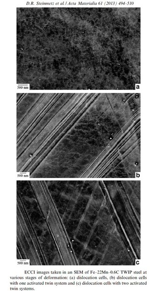
Acta Materialia 61 (2013) 494-510
David R. Steinmetz, Tom Jäpel, Burkhard Wietbrock, Philip Eisenlohr, Ivan Gutierrez-Urrutia, Alireza Saeed–Akbari, Tilmann Hickel, Franz Roters, Dierk Raabe
Revealing the strain-hardening behavior of twinning-induced plasticity steels: Theory, simulations, experiments
Acta Materialia 61 (2013) 494 ab initio [...]
PDF-Dokument [1.8 MB]
Here we present a multiscale dislocation density-based constitutive model for the strain-hardening behavior in twinning-induced plasticity (TWIP) steels. The approach is a physics-based
strain rate- and temperature-sensitive model which reflects microstructural investigations of twins and dislocation structures in TWIP steels. One distinct advantage of the approach is that the
model parameters, some of which are derived by ab initio predictions, are physics-based and known within an order of magnitude. This allows more complex microstructural information to be
included in the model without losing the ability to identify reasonable initial values and bounds for all parameters.
Dislocation cells, grain size and twin volume fraction evolution are included. Particular attention is placed on the mechanism by which new deformation twins are nucleated, and a new formulation
for the critical twinning stress is presented. Various temperatures were included in the parameter optimization process. Dissipative heating is also considered. The use of physically justified
parameters enables the identification of a universal parameter set for the example of an Fe–22Mn–0.6C TWIP steel.
JOM, Vol. 65, No. 9, 2013
Coupling of Electron Channeling with EBSD: Toward the Quantitative Characterization of Deformation Structures in the SEM
I. GUTIERREZ-URRUTIA,S. ZAEFFERER, D. RAABE
JOM Vol. 65 No. 9 2013 Overview Electron[...]
PDF-Dokument [812.0 KB]
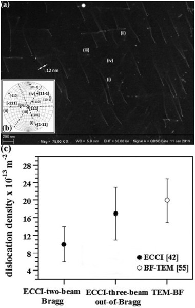
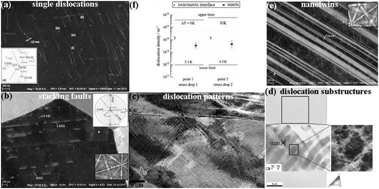
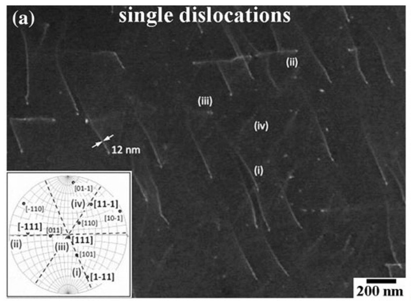
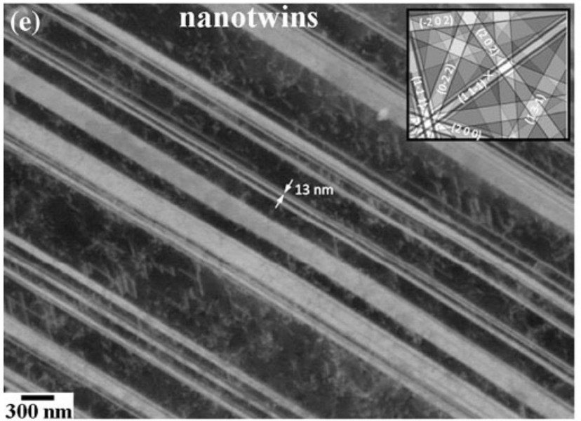
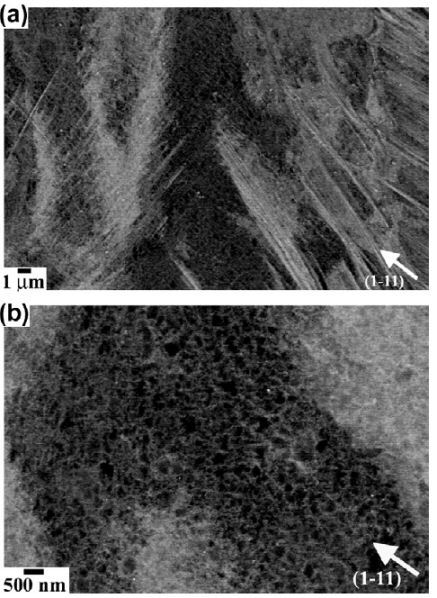
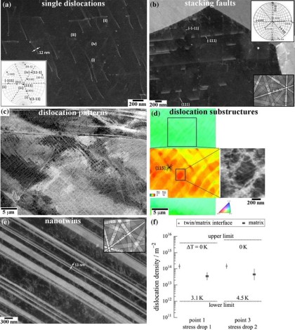 Electron Channeling Contrast Imaging: Application examples of the ECCI technique: (a) characterization of single dislocations, (b) stacking faults, (c–d) dislocation substructures, and (e) nanotwins; (f) measurement of dislocation densities
The coupling of electron channeling contrast imaging (ECCI) with electron
backscatter diffraction (EBSD) provides an efficient and fast approach to
perform ECCI of crystal defects, such as dislocations, cells, and stacking
faults, under controlled diffraction conditions with enhanced contrast. From a
technical point of view, the ECCI technique complements two of the main
electron microscopy techniques, namely, EBSD and conventional diffraction based transmission electron microscopy. In this review, we provide several
application examples of the EBSD-based ECCI approach on microstructure
characterization, namely, characterization of single dislocations, measurement
of dislocation densities, and characterization of dislocation substructures
in deformed bulk materials. We make use of a two-beam Bloch wave approach
to interpret the channeling contrast associated with crystal defects. The approach captures the main features observed in the experimental contrast
associated with stacking faults and dislocations.
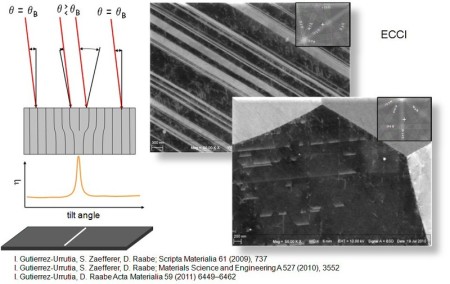
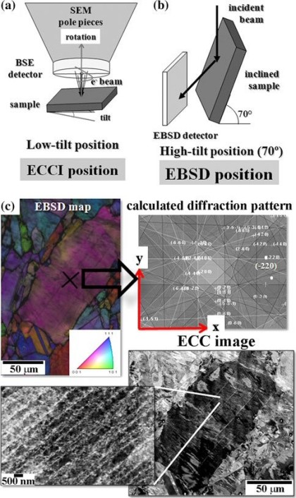
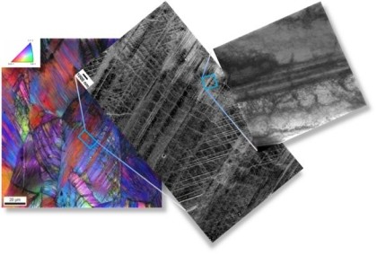
More specific, we use a new approach to electron channelling contrast imaging (ECCI), referred to as “controlled ECCI”, or cECCI. This method improves the existing ECCI method in a way that it uses EBSD to determine the crystal orientation. Based on this orientation measurement the optimum sample alignment for obtaining good channelling contrast is calculated. A dedicated eucentric goniometer stage is then used to move the sample into the calculated position for imaging of dislocations and other crystal defects in the SEM. The approach offers excellent opportunities for the efficient quantification of substructure features at a large field of view that were not accessible so far to SEM characterization. It can be combined with EBSD maps so that we are now capable of conducting detailed microstructure quantification mappings of orientations together with its dislocation substructure in the same experiment. Time consuming TEM investigations of dislocation structures that provide a small field of view and that are affected by the thin slice preparation typical of TEM thus may become obsolete in a number of cases.
I. Gutierrez-Urrutia, D. Raabe, Dislocation and twin substructure evolution during strain hardening of an Fe–22 wt.% Mn–0.6 wt.% C TWIP steel observed by electron channeling contrast imaging, Acta Materialia 59 (2011) 6449–6462
I. Gutierrez-Urrutia, S. Zaefferer, D. Raabe: The effect of grain size and grain orientation on deformation twinning in a Fe–22 wt.% Mn–0.6 wt.% C TWIP steel, Mater. Sc. Engin. A 527 (2010) 3552-3560
I. Gutierrez-Urrutia, S. Zaefferer, D. Raabe: Electron channeling contrast imaging of twins and dislocations in twinning-induced plasticity steels under controlled diffraction conditions in a scanning electron microscope, Scripta Mater. 61 (2009) 737-740
I. Gutierrez-Urrutia, D. Raabe: Viewpoint Set no. 50: Twinning Induced Plasticity Steels: Grain size effect on strain hardening in twinning-induced plasticity
steels,
Scripta Materialia, Volume 66, Issue 12, June 2012, Pages 992–996
 ECCI Analysis on TWIP steel
 Dislocations in the SEM by using ECCI and EBSD (Gutierrez-Urrutia, Zaefferer, Raabe: Scripta Mater. 61 (2009) 737)
Acta Materialia 59 (2011) 6449-6462
Dislocation and twin substructure evolution during strain hardening of an Fe–22 wt.% Mn–0.6 wt.% C TWIP steel observed by electron channeling contrast imaging
I. Gutierrez-Urrutia, D. Raabe
Acta Materialia 59 (2011) 6449 ECCI TWIP[...]
PDF-Dokument [2.5 MB]
 Acta Materialia 59 (2011) 6449 Dislocation and twin substructure evolution during strain hardening of an Fe–22 wt.% Mn–0.6 wt.% C TWIP steel observed by electron channeling contrast imaging I. Gutierrez-Urrutia, D. Raabe
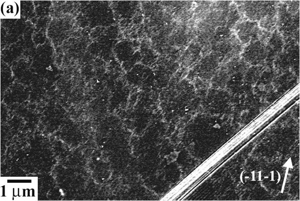
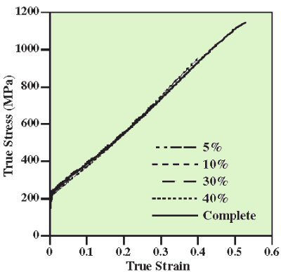
High-manganese steels have received much interest in recent years due to their outstanding mechanical properties combining high strength and ductility. This property profile is attributed to their high strain hardening capacity. High-manganese steels are typically austenitic steels, i.e. face-centered cubic (fcc) alloys, with a high Mn content (above 20% wt.%) and additions of elements such as carbon (<1 wt.%), silicon (<3 wt.%) and aluminum (<10 wt.%). This steel grade exhibit different hardening mechanisms, such as transformation-induced plasticity (TRIP), twinning-induced plasticity (TWIP) or microband-induced plasticity (MBIP). The activation of these mechanisms is strongly dependent on the stacking fault energy. TRIP is observed in very low stacking fault steels (below 20 mJ / m^2) and is associated with the transformation of austenite (fcc phase) into epsilon-martensite (hexagonal close-packed phase), which in turn further acts as nucleus of a'-martensite (body-centered cubic or tetragonal phase). TWIP is observed in medium stacking fault energy steels (20–40 mJ/ m^2) and is characterized by the formation of deformation twins with nanometer
thickness. MBIP has been recently reported in steel grades with high stacking fault energy (90 mJ / m^2) and is attributed to the formation of microbnds, which are in-grain shear zones that are confined by geometrically necessary boundaries or conventional grain boundaries. These microstructure features (e-martensite plates, deformation twins and microbands) lead to a remarkable variety of strain hardening phenomena as they all act as effective obstacles for dislocation glide. High-manganese TWIP steels are characterized by a hierarchical microstructure refinement that includes complex dislocation and twin substructures, and their interactions. Although there are some previous studies on the strain hardening behavior in TWIP steels, the details of the underlying kinetics of the substructure evolution and its correspondence to the stress–strain
and strain hardening evolution is not yet fully understood. Most of these works analyze strain hardening in terms of a dislocation mean free path (MFP) approach,
focusing essentially on a single microstructure parameter, namely,
the twin spacing. These works attribute the high strain hardening rate at intermediate strains (0.1–0.2 true strain) to twin spacing refinement. The increasing density of deformation
twin boundaries and the strong effect they
have on dislocation glide leads to the so-called “dynamic Hall–Petch effect”. However, our analysis reveals that the deformed microstructure of these alloys is too complicated to be
reduced to a single microstructure parameter and,
therefore, a detailed analysis of the contribution of dislocation and twin substructures, as well as their interactions, to strain hardening is required.
One important limitation in the characterization of TWIP steels is the complexity of the microstructure, which involves features of different length scales: deformation twins with
thicknesses of some tens of nanometers and dislocation substructures extending over several micrometers. As a consequence of this scale discrepancy, quantitative microstructure
characterization by
conventional electron microscopy techniques such as electron backscatter diffraction (EBSD) or transmission electron microscopy (TEM) is limited due to the angular resolution (EBSD)
and the small field of view (TEM), respectively. In Here, therefore, we make use of electron channeling contrast imaging (ECCI), which is conducted in a scanning electron microscope
(SEM), to perform a quantitative characterization of the deformation microstructure of TWIP steel. The ECCI technique has been established as an excellent tool for examining
complex deformation microstructures of metallic materials, revealing
microstructure features such as deformation twins, stacking faults and complex dislocation arrangements from a wide field of view directly in the SEM. The reason for the recent
improvement in the ECCI technique lies in its combination with EBSD. This allows us to efficiently identify optimum contrast conditions and, therefore, produce ECCI images of crystal
defects under controlled diffraction
conditions. Here, we study the kinetics of the substructure evolution and its correspondence to the strain hardening
evolution of an Fe–22 wt.% Mn–0.6 wt.% C TWIP steel during tensile deformation by means of electron channeling
contrast imaging (ECCI) combined with electron backscatter diffraction (EBSD). The contribution of twin and
dislocation substructures to strain hardening is evaluated in terms of a dislocation mean free path approach
involving several microstructure parameters, such as the characteristic average twin spacing and the dislocation
substructure size. The analysis reveals that at the early stages of deformation (strain below 0.1 true strain) the dislocation substructure provides a high strain hardening rate with hardening coefficients of about G/40 (G is the shear modulus). At
intermediate strains (below 0.3 true strain), the dislocation mean free path refinement due to deformation
twinning results in a high strain rate with a hardening coefficient of about G/30. Finally, at high strains
(above 0.4 true strain), the limited further refinement of the dislocation and twin substructures reduces the
capability for trapping more dislocations inside the microstructure and, hence, the strain hardening decreases.
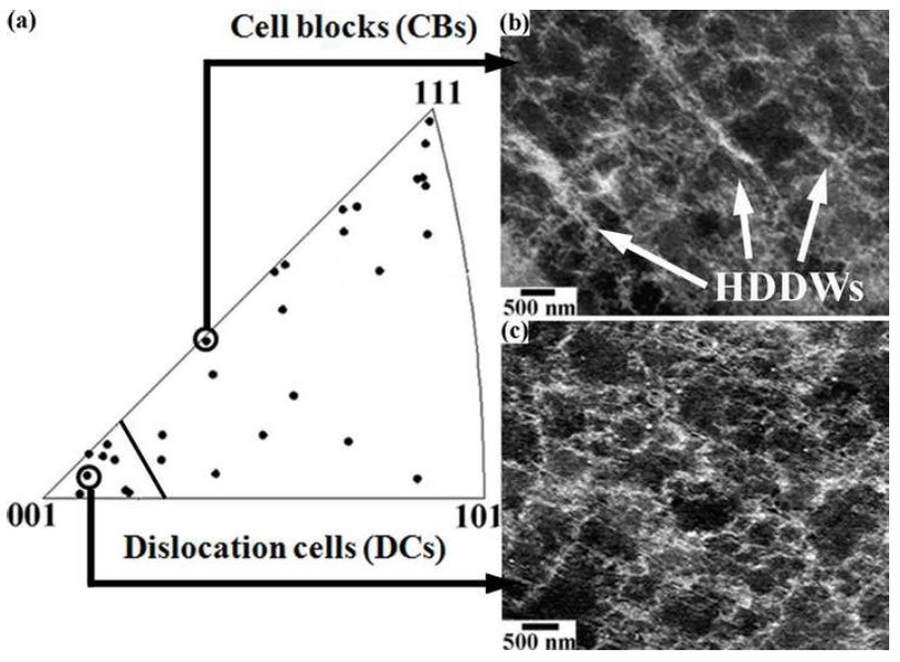
Grains forming dislocation cells develop a self-organized and dynamically refined dislocation cell structure which follows the similitude principle but with a smaller similitude constant than that found in medium to high stacking fault energy alloys. We
attribute this difference to the influence of the stacking fault energy on the mechanism of cell
formation.
We study hydrogen embrittlement in Fe–18Mn–1.2%C (wt.%) twinning-induced plasticity steel, focusing on the influence of deformation twins on hydrogen-assisted cracking.
Acta-Mater-hydrogen-induced-cracking-201[...]
PDF-Dokument [4.0 MB]
Here we study the kinetics of the deformation structure evolution and its contribution to the strain hardening of a Fe–30.5Mn–2.1Al–1.2C (wt.%) steel during tensile deformation by means of trans
2012-Acta FeMnAlC-multi-strain-hardening[...]
PDF-Dokument [1.8 MB]
 High Mn steel characterized by EBSD, ECCI and TEM (Materials Science and Engineering A 527 (2010) 3552).
 Application of the ECCI method to weight reduced TRIPLEX steels.
Here we present a multiscale dislocation density-based constitutive model for the strain-hardening behavior in twinning-induced plasticity (TWIP) steels. The approach is a physics-based strain rate- a
Acta-Materialia-Vol-61-2013-modeling-TWI[...]
PDF-Dokument [1.8 MB]