Shear-induced mixing governs co-deformation of crystalline-amorphous nanolaminates
Deformation of ductile crystalline-amorphous nanolaminates is not well understood due to the complex interplay of interface mechanics, shear banding and deformation-driven chemical mixing. Here we present indentation experiments on 10 nm nanocrystalline Cu / 100 nm amorphous CuZr model multilayers to study these mechanisms down to the atomic scale. By using correlative atom probe tomography and transmission electron microscopy we find that crystallographic slip bands in the Cu layers coincide with non-crystallographic shear bands in the amorphous CuZr layers. Dislocations from the crystalline layers drag Cu atoms across the interface into the CuZr layers. Also, crystalline Cu blocks are sheared into the CuZr layers. In these sheared and thus Cu enriched zones the initially amorphous CuZr layer is rendered into an amorphous plus crystalline nanocomposite.
Metallic crystalline-amorphous nanolaminate composites were reported to be both ductile and strong [1-8]. The reason for this mechanical response is not understood since glassy compounds usually fail already at low strains [9-11].
For identifying the co-deformation mechanisms in such composites, we synthesized and indented model nanolaminates consisting of nanocrystalline Cu and amorphous Cu54Zr46. The alternating layers were deposited on Si (100) wafers by magnetron sputtering using pure Cu and Zr targets (99.99 at.%) [12]. The base pressure was below 4×10⁻⁵ Pa and the processing pressure was 4×10⁻¹ Pa Ar. The thickness of the crystalline Cu and amorphous CuZr layers was 10 and 100 nm, respectively. The total thickness of the Cu/CuZr multilayer stack with a cap CuZr layer on the top was ~1200 nm. The Cu nanocrystals had a <111> fiber texture, measured by XRD. The nanolaminates were indented with a 10 g Vickers indenter for 10s (Fig.1a).
To study nanostructural and atomic-scale chemical deformation effects at the same position we performed a joint analysis by transmission electron microscopy (TEM) and Atom Probe Tomography (APT) [17-19]. TEM lamellae of ≈100 nm thickness were prepared by an in-situ lift-out method and focused-ion-beam (FIB) milling. A 200 kV Jeol JEM-2200FS TEM was used for high-resolution TEM and nano-beam diffraction (NBD). For the correlative TEM-APT analysis, tip-shaped specimens containing deformation shear bands were cut by site-specific preparation, mounted onto an electro-polished bisected TEM Cu grid, and thinned by annular FIB milling{Miller, 2007 #1524}. APT was performed with a local electrode atom probe (LEAP 3000X HR). Samples were analyzed at 60 K, applying 532 nm wavelength 10 ps laser pulses of 0.4 nJ with at a repetition rate of 250 kHz. The datasets were reconstructed using the software IVAS 3.6.6 (CAMECA Instruments) [13,14].
APT analyses of as-deposited samples were performed with the tip evaporation direction both, perpendicular and parallel to the CuZr/Cu interfaces. The Cu concentration is 54.2 ± 0.3 at.% in the amorphous CuZr layers and 99.2 ± 0.5 at.% in the Cu layers. The laminates contain traces of impurity oxygen from sputtering [15]. The width of interfaces oriented perpendicular to the analysis direction is ~1.5 nm for the CuZr/Cu interfaces and ~4 nm for the Cu/CuZr interfaces. This difference is due to ion trajectory aberrations at the interface when the tip is evaporated from the CuZr layer with a lower field of evaporation to the Cu layer with a higher field of evaporation, resulting in an apparent interfacial width compression, and, vice versa, to an apparent interfacial width expansion for the opposite layer evaporation sequence. From measurements with the interfaces parallel to the evaporation direction, the interfaces were found to be more symmetric with a width of ~3 nm. This high value is due to local magnification [16] and interface roughness.
After indentation, sharp shear bands around the pile-up regions are observed, Fig. 1a-c. The Cu layers are not significantly reduced in thickness in most pile-up regions. However, they are deformed to a thickness of ~2.5 nm inside the shear bands. Fig. 1d-e show the correlative TEM and APT analysis. The area in the bright field (BF) TEM micrograph of an APT specimen highlighted in yellow is the volume containing a shear band analyzed by APT, Fig. 1d. The yellow lines mark a region representing the volume investigated by APT although the actual APT data in Fig. 1e were taken from a slightly different region in the same sample. The white rectangles in Fig 1d indicate regions from which NBD patterns were acquired. They show crystalline diffraction spots in the Cu region and an amorphous halo in the CuZr region. Fig. 1e reveals the atomic composition of the sheared region taken by APT together with the crystallographic orientation obtained from TEM. It shows that the {111} planes of the Cu are parallel to the interface plane of the shear band.
Fig. 1c-e reveal zones with a large and very sharp, abruptly sheared Cu layer offset >30nm. The layer is not completely disconnected from the sheared region though. Instead, it is heavily deformed at a 70.5° tilt angle to the interface plane, which corresponds to the {111}{Sauvage, 2009 #499} planes in Cu. In the shear band region, the Cu layers are subjected to a huge true shear strain of 4.0 ± 0.2, as calculated from the layer displacement. The observations indicate dislocation slip on {111} planes in the Cu. The large displacement (>30nm) of the sheared and fragmented Cu layer shown in Fig. 1e suggests that large numbers of Cu dislocations accommodate the shear inside the crystalline phase, extending it across the Cu/CuZr interface into the initially amorphous layer.
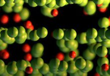
The 60 at.% iso-concentration Cu surface (Fig.2a) indicates that chemical mixing between the crystalline and amorphous phase has occurred along the shear offset of the Cu layer. Several regions in this zone were probed for composition (Fig. 2b-d). A non-sheared amorphous region is shown for reference in Fig. 2b. Although this amorphous region was also near the shear band zone it does not indicate any remarkable chemical fluctuations compared to the as-deposited amorphous CuZr layer (Cu 55.1±2.1 at.%, Zr 44.9 ±2.1 at.% in average). In contrast, the concentrations mapped across the shear band that penetrated both, the Cu layer and the amorphous zone below it (Fig 2c), show strong Cu enrichment (~68 at.% in average) of ~2.5 nm thickness in the sheared portion of the CuZr layer. The concentration and the interfacial width of the remaining Cu layer does not change (Fig 2d) compared to the as-deposited state. This indicates that deformation induced mixing occurs only within a narrow region (~2.5 nm) inside the shear band [20,21].
The sampling region marked by red lines in Fig. 2a (size: 9×32×32 nm3) represents the mixing zone inside the shear band, where Cu atoms have been displaced out of the crystalline Cu layer and into the initially amorphous CuZr region. We use the position of the original Cu layer as coordinate start and the longitudinal axis corresponds to the dislocation slip direction inside the crystalline Cu. Along the shear direction, the chemical concentration of Cu varies from 60 at.% to 88 at.% where the average number of atoms in each sampling bin (0.3 nm width) is ~3000. The mean displacement of the Cu atoms in this shear region is calculated by , where is the Cu concentration in one sampling bin (9×32×0.3 nm3), is the Cu concentration in the CuZr layer in the as-deposited state, is the number of atoms in the ith bin, and is the distance between the ith bin and the original Cu layer position. is the number of displaced Cu atoms inside the ith bin. This estimate gives a mean shear displacement of the Cu atoms stemming from the crystalline layer of 11.75±1.50 nm into the amorphous CuZr region. For the time elapsed during this displacement we use the indentation time (t=10s) as an upper bound, knowing that shear band events occur more abruptly. The associated pseudo diffusion coefficient is ≈2.30×10⁻¹⁴ cm2/s, which is 24 orders of magnitude above Cu self-diffusion at room temperature [22]. We use Cu self-diffusion as an approximation as no literature is available about the diffusion coefficient of Cu in amorphous CuZr.
To understand the observed deformation-induced atomic mixing, we probe several compositional profiles across the Cu enriched region inside the shear band. Several regions across the Cu layer and outside the shear band were also analyzed (table 1) for reference. The interface width here is defined as the average spacing of the two interfaces pertaining to one Cu layer. This analysis reveals that mixing in the sheared regions of the Cu layer is caused by the shear band running through it: In this mixing zone the Cu concentration varies from 64.6 at.% to 95.4 at.% within a narrow shear layer thickness range of only 2~3 nm. In contrast, no excess Cu is found above that shear band, i.e. mixing is confined to a very narrow zone. The accelerated transport of Cu from the Cu layer into the CuZr region (see estimate of the diffusion coefficient) occurs only inside the shear band. Regions outside the shear band have the same interface width and concentration profiles as the as-deposited layers, i.e. they do not undergo deformation-driven mixing.
Fig. 3 shows high-resolution TEM (HRTEM) images obtained from the sheared offset region of shear bands in the 100 nm CuZr/10 nm Cu multilayer specimen. Attention is placed on the mixing inside the initially amorphous CuZr zone, caused by atoms that are sheared out of the Cu layer into the metallic glass. Several spots along the shear band were selected for structural analysis. Fig. 3(b) shows a HRTEM image and NBD patterns along the pathway of a shear band (spots 2-7) and, as reference, from a region inside the undeformed amorphous layer (spot 1). The sizes of the circles indicate the diameter of the diffraction aperture. NBD at spot 1 shows no crystalline diffraction but only a halo typical of an amorphous structure. NBD spots 2 and 7 are given as references for dominantly crystalline material associated to non-sheared portions of the Cu layers close to the shear band.
Surprisingly, some of the NBD patterns taken along the shear band penetrating the initially amorphous CuZr layer show both, an inner halo ring (amorphous material) as well as some weak discrete diffraction spots (crystalline material) outside of the inner halo ring (arrows, NBD spots 3,4,6). This means that the initially amorphous CuZr layer has been rendered into an amorphous plus crystalline composite by the shear band and the associated mixing as proven by the diffraction spots 3, 4, and 6.
This indicates that the crystalline diffraction spots stem either from jointly sheared Cu fragments of the crystalline layer or from a portion inside the initially amorphous regions that crystallized due to the increase in Cu content. The lattice parameter of d(111)=0.209 nm, determined from FFT diffraction patterns, supports the possibility that compact nanocrystalline Cu portions might have been displaced by the shear band into the initially amorphous CuZr zone.
The absence of clearly visible crystalline diffraction spots in the NBD pattern taken at spot 5 suggests that this region remained amorphous. Fig. 3c,d show a similar shear region. Here a clearly crystalline structure containing a very high dislocation content can be observed inside the initially amorphous CuZr zone.
A number of very similarly sheared and, hence, mixed regions have been observed and characterized as demonstrated in the attached supplemental material. Fig. SM1 shows three APT data sets obtained from the 100 nm CuZr/10 nm Cu multilayer system after indentation with a 10 g load at various strains (a-c). The local strains were obtained by quantifying the offset among neighboring layers. 1D-Cu concentration profiles taken perpendicular through the shear banded regions inside the originally amorphous layers are shown in Fig. SM1 (d) and marked by arrows.
Following a similar motivation several related studies on deformation-driven mixing were conducted in the field of severe plastic deformation using electron microscopy and APT [20,23-28]. In these works several types of crystalline systems, often with small mutual solubility, were exposed to very large strains via ball milling, high pressure torsion, or wire drawing. The difference is that here we study co-deformation of a crystal / metallic glass nanocomposite and consider the mixing mechanisms associated with the early stages of the deformation process rather than after severe deformation. Also, the shear banded regions are here probed using correlative TEM-APT methods [18].
In Fig. 4 we propose a mechanism for the deformation and alloying process in the nanolaminate. Previous work showed that the yield stress of nanocrystalline Cu (grain size 10 nm, >3000 MPa) is above that of amorphous CuZr (~2500 MPa) [29]. Thus, it is plausible that plastic deformation of the nanolaminate starts by initiating shear transformation zones (STZs) [30] inside the amorphous CuZr layers and developing them into shear bands, Fig. 4a [9-11]. This leads to stress localization when the band impinges the crystalline Cu, activating dislocation nucleation at the amorphous/crystalline interface. The Cu dislocations glide on {111} planes, Fig. 4b. These dislocations, when crossing from the Cu layer into the amorphous CuZr layer [31], cause a displacement which is an integer multiple of the Cu Burgers vector, Fig. 4c. The density of mobile dislocations carrying the shear band through the crystalline Cu layer can be calculated by , where =4.03±0.18 is the local offset shear strain; =0.255 nm is the Burgers vector of Cu; and =10 nm/sin70.5º=10.64 nm is the mean path of dislocations gliding through the Cu layer into the CuZr/Cu interface.
This estimate gives a mobile dislocation density of ~1.48×10¹⁸ m-2 inside the Cu shear zone which is 2-3 orders of magnitude above that in heavily deformed Cu [32]. However, this value does not reflect a stored dislocation density. These dislocations are formed at one CuZr/Cu hetero-interface and are absorbed at the opposite one, Fig. 4d. Similar observations on the propagation of shear bands across hetero-interfaces in a Zr-Ti-Cu-based crystal-metallic glass composite were made by Pekarskaya et al. [31].
In cases where crystalline portions from the Cu are displaced into the amorphous layer (Fig 3b), very high dislocation densities are found, Fig. 3c,d. This observation supports the view of complete crystalline portions being sheared out of the Cu since crystallization due to Cu enrichment would lead to undistorted crystals.
In conclusion, we observe co-deformation by shear-dislocation shuffling in crystalline (Cu) / amorphous (CuZr) nanolaminates at scales down to the atomic scale. The mechanism can explain co-deformation and shear-induced mixing phenomena in the present context. The mechanism is characterized as follows: (i) Local thinning of the Cu phase can be attributed to the high density of gliding dislocations. (ii) Cu atoms are dragged across the hetero-interface when dislocations release their shear step into the amorphous CuZr phase (Fig. 4e). This leads to intense mixing among the layers inside 2-3 nm narrow shear bands. The Cu enrichment can lead to crystallization. (iii) Besides dislocation driven mixing, nm-sized compact portions of crystalline Cu are displaced into the amorphous phase (Fig. 3b-d). This means that the intense chemical intermixing during trans-phase co-deformation includes both, individual solute transport via dislocations and collective shear of tiny crystalline portions from the crystalline into the amorphous phase. In the shear banded Cu-enriched zones the initially amorphous CuZr forms an amorphous plus crystalline nanocomposite.
References:
- T.G. Nieh, T.W. Barbee, and J. Wadsworth, Scripta Mater. 41, 929 (1999).
- D. C. Hofmann, J.-Y. Suh, A. Wiest, G. Duan, M.-L. Lind, M.D. Demetriou, and W.L. Johnson, Nature 451, 1085 (2008).
- C. C. Hays, C. P. Kim, and W. L. Johnson, Phys. Rev. Lett. 84, 2901 (2000).
- H. Huang and F. Spaepen, Acta Mater. 48, 3261 (2000)
- T. G. Nieh, J. Wadsworth, C. T. Liu, T. Ohkubo, and Y. Hirotsu, Acta Mater. 49, 2887 (2001).
- J.R. Greer and J.T.M. De Hosson, Prog. Mater. Sci. 56, 654 (2011).
- M. W. Chen, A. Inoue, W. Zhang, and T. Sakurai, Phys. Rev. Lett. 96, 245502 (2006).
- Y.M. Wang, J. Li, A.V. Hamza, and T.W. Barbee, Proc. Natl. Acad. Sci. USA 104, 11155 (2007).
- C. A. Schuh, T. C. Hufnagel, and U. Ramamurty, Acta Mater. 55, 4067 (2007).
- J.-Y. Kim , D. Jang , and J. R. Greer, Adv. Funct. Mater. 21, 4550 (2011).
- I. Kaban, P. Jovari, V. Kokotin, O. Shuleshova, B. Beuneu, K. Saksl, N. Mattern, J. Eckert, and A.L. Greer, Acta Mater. 61, 2509 (2013).
- T. Gebhardt, D. Music, M. Ekholm, I.A. Abrikosov, J. von Appen, R. Dronskowski, D. Wagner, J. Mayer, and J.M. Schneider, Acta Mater. 59, 1493 (2011)
- M. K. Miller and K. F. Russell, Ultramicroscopy 107, 761 (2007).
- K. Thompson, D. Lawrence, D. J. Larson, J. D. Olson, T. F. Kelly, and B. Gorman, Ultramicroscopy 107, 131 (2007).
- J.M. Schneider, B. Hjörvarsson, X. Wang, and L. Hultman, Appl. Phys. Let. 75, 3476 (1999).
- P. Bas, A. Bostel, B. Deconihout, and D. Blavette, Appl. Surf. Sci. 87, 298 (1995).
- P. J. Felfer, T. Alam, S. P. Ringer, and J. M. Cairney, Microsc. Res. Techn. 75, 484 (2012).
- M. Herbig, D. Raabe, Y. J. Li, P. Choi, S. Zaefferer, and S. Goto, Phys. Rev. Let. 112, 126103 (2014).
- M. J. Duarte, J. Klemm, S. O. Klemm, K. J. J. Mayrhofer, M. Stratmann, S. Borodin, A. H. Romero, M. Madinehei, D. Crespo, J. Serrano, S. S. A. Gerstl, P. P. Choi, D. Raabe, and F. U. Renner, Science 341 (2013) 372.
- D. Raabe, P. P. Choi, Y. J. Li, A. Kostka, X. Sauvage, F. Lecouturier, K. Hono, R. Kirchheim, R. Pippan and D. Embury, MRS Bulletin 35, 982 (2010).
- D. Raabe, S. Ohsaki, and K. Hono, Acta Materialia 57, 5254 (2009).
- K. Maier, Phys Status Solidi A 44, 567 (1977).
- X. Quelennec, A. Menand, J.M. Le Breton, R. Pippan, and X. Sauvage, Phil. Mag 90, 1179 (2010).
- M. Wang, N.Q. Vo, M. Campion, T.D. Nguyen, D. Setman, S. Dillon, P. Bellon, and R.S. Averback, Acta Mater. 66, 1 (2014).
- X. Sauvage, P. Jessner, F. Vurpillot and R. Pippan, Scripta Mater. 58, 1125 (2008).
- M. Wang, R. S. Averback, P. Bellon, and S. Dillon, Acta Materialia 62, 276 (2014).
- Y.J. Li, P. Choi, C. Borchers, S. Westerkamp, S. Goto, D. Raabe, and R. Kirchheim, Acta Mater. 59, 3965 (2011).
- Y.Z. Chen, A. Herz, Y.J. Li, C. Borchers, P. Choi, D. Raabe, and R. Kirchheim. Acta Mater. 61, 3172 (2013).
- J. Y. Zhang, G. Liu, S. Y. Lei, J. J. Niu, and J. Sun, Acta Mater 60, 7183 (2012).
- J. S. Langer, Scripta Mater 54, 375 (2006).
- E. Pekarskaya, C.P. Kim, and W.L. Johnson, J. Mater. Res. 16, 2513 (2001).
- M. R. Staker and D. L. Holt, Acta Metall 20, 569 (1972).
 SEM view of CuZr/Cu multilayers after Vickers indentation with a load of 10g. b) Cross-sectional view of shear bands beneath an indent.")
 Two different 3D Cu iso-concentration surface views and a schematic of a portion of the same APT measurement presented in Fig. 1 containing a shear band.")


PRL 113, 035501 (2014) PHYSICAL REVIEW LETTERS
Guo Phys Rev Lett 113.035501 CuZr metal-[...]
PDF-Dokument [2.1 MB]
Acta Materialia 80 (2014) 94–106
Acta Materialia 80 (2014) 94 Nanolaminat[...]
PDF-Dokument [3.9 MB]